

silicon photonics
PsiQuantum Targets AI Data Center Networks with Silicon-Photonic Optical Switching
Disclaimer: ChatGPT was used extensively for research contained in this article.
……………………………………………………………………………………………………………………………………..
Introduction:
As AI workloads expand and AI clusters grow, the networks connecting GPUs and other accelerators are becoming an increasingly important constraint on performance, power consumption and cost. Optical circuit switching (OCS) offers one way to improve connectivity by establishing direct optical paths between network ports without converting optical signals into electrical signals for packet-by-packet switching.
On October 28th, PsiQuantum [1.] unveiled an 8×8 optical circuit-switching demonstration built on its low-loss silicon-photonics platform, originally developed for quantum computing. The company reports promising laboratory results and is sharing demonstration samples with selected prospective customers. The key question is whether this technology can scale into a commercially competitive product for AI data centers.
Note 1. PsiQuantum was founded on the premise that photonic qubits, together with leverage of mature semiconductor manufacturing processes, would provide the fastest path to commercially useful, fault-tolerant quantum computers. Today, PsiQuantum builds tens of thousands of wafers of quantum chips in a tier-1 foundry, operates cryogenic cabinets supporting hundreds of chips, advances fault-tolerant algorithm development to solve critical problems across industries, and is developing a modular quantum computing platform designed to increase capability and scale. Each milestone brings us closer to delivering commercially useful quantum computing. The company’s headquarters is in Palo Alto, CA. Source: PsiQuantum
Optical Circuit Switching (OCS) for AI Data Centers:
Large AI clusters rely on high-speed interconnects to move model parameters, gradients, activations and other data among processors. Network congestion, communication overhead and power consumption can limit how effectively expensive accelerators are utilized. Ethernet and InfiniBand networks rely primarily on packet switches to route traffic dynamically.
OCS takes a different approach: it establishes direct optical connections between selected ports, allowing light to pass through the switching fabric without optical-electrical-optical conversion at the switch. This approach can complement conventional packet switching in AI clusters, particularly when communication patterns are predictable or recurring. A network controller can establish optical paths between selected racks or groups of accelerators, while packet switches handle traffic requiring flexible, fine-grained routing.
OCS is therefore a potential complement to conventional switching fabrics, not a wholesale replacement for Ethernet or InfiniBand. Its benefits depend on network architecture, traffic patterns, connection utilization and the overhead of reconfiguring optical paths.
Here’s an illustration of optical circuit switching in an AI data-center network. Optical circuit switches establish direct optical paths between selected network ports, complementing conventional packet switching. Conceptual illustration—not a depiction of PsiQuantum’s specific product or a verified implementation.
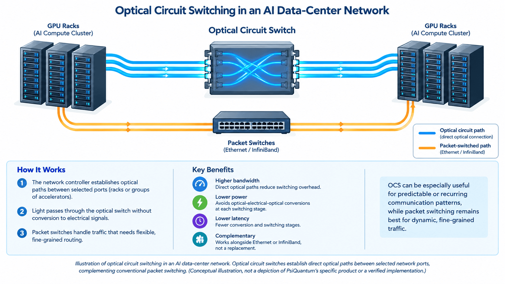
Image Credit: ChatGPT
………………………………………………………………………………………………………………………………………………………………………………………………………….
PsiQuantum’s 8×8 Demonstration:
PsiQuantum describes its first publicly disclosed device as a strictly non-blocking 8×8 switch, meaning any input can connect to any output. The silicon-photonic device operates without moving parts.
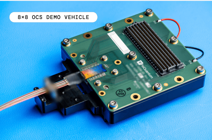
The company reports the following laboratory results:
| Parameter | Company-reported result |
|---|---|
| Switch configuration | 8×8 |
| Typical insertion loss | 1.2 dB |
| Crosstalk | 40 dB |
| Reconfiguration time | Less than 3 ms |
| Optical amplification | Not required |
Source: PsiQuantum, October 28, 2026. These are company-reported laboratory results, not independently verified benchmarks.
“This opportunity exists because we chose to solve the hardest scaling problems at the beginning of our roadmap to utility-scale quantum computing,” said Victor Peng, Chief Executive Officer of PsiQuantum. “As AI computing pushes infrastructure to its limits, we now have an opportunity to put our state-of-the-art technology to work today while continuing toward our ultimate goal: building and deploying the world’s first useful, fault-tolerant quantum computers.”
“AI is driving extraordinary growth in the scale and complexity of computing infrastructure, and optics will play an increasingly important role in enabling that growth,” said Rob Soderbery, Executive Vice President at PsiQuantum. “PsiQuantum has spent nearly a decade developing silicon photonics against some of the most demanding requirements imaginable. What we are demonstrating today is that this platform can deliver exceptional performance for optical circuit switching for AI computing.”
PsiQuantum has also developed barium titanate (BTO) integration at the 300mm wafer scale and uses a 64×64 BTO switch in its quantum systems. BTO is not required for the demonstration vehicle or initial products announced today, highlighting the performance of the underlying silicon photonics platform while preserving an additional path to faster, more advanced future products.
………………………………………………………………………………………………………………………………………………………………………………………………
EE Analysis:
Insertion loss measures the optical power lost as a signal passes through the switch. The reported 1.2 dB figure suggests that relatively little power is lost in the device itself.
Crosstalk measures unwanted signal leakage between channels, while reconfiguration time indicates how quickly the switch can establish a new connection arrangement.
A switching time below 3 milliseconds could support some scheduled or recurring AI communication patterns. However, suitability depends on workload characteristics, connection-management overhead and how effectively established paths are utilized.
PsiQuantum says its silicon-photonics platform leverages semiconductor manufacturing at Global Foundries in New York. It has also developed barium titanate integration at 300-mm wafer scale, but the company says this technology is not required for the demonstrated switch or its initial products. Its 8×8 device should therefore be judged on its own reported performance, rather than the potential capabilities of future products.
……………………………………………………………………………………………………………………………………………………………………………………………………………………………………………………………………..
Google Provides a Production-Scale Benchmark:
Optical circuit switching is already deployed in hyperscale data-center networks. Google’s Jupiter architecture provides an important real-world comparison.
In a 2022 ACM SIGCOMM paper, Google engineers described how Jupiter evolved from a conventional Clos network toward a direct-connect topology between aggregation blocks. Its Apollo optical circuit switches use micro-electromechanical systems (MEMS) mirrors to steer light between fiber ports. A software-defined networking (SDN) control plane dynamically adjusts the network’s logical topology and traffic paths, while packet switches continue to handle traffic routing.
Google’s paper reported that the broader evolution of Jupiter delivered a fivefold increase in network speed and capacity, a 30% reduction in capital expenditure and a 41% reduction in power consumption while serving live production traffic. These improvements resulted from the overall architecture—including optical switching, traffic engineering and network-management changes—not from the optical switches alone.
The distinction is important. Google has demonstrated production-scale OCS integrated with network control and traffic engineering. PsiQuantum has reported promising component-level results from an 8×8 silicon-photonic laboratory demonstration. The two systems also use different switching technologies.
Google’s experience nevertheless demonstrates that OCS can deliver substantial benefits when integrated into a carefully engineered network. PsiQuantum’s challenge is to show that its silicon-photonics approach can provide comparable practical value at scale.
The Commercial Test:
PsiQuantum must now demonstrate that its reported performance can be maintained in larger configurations and integrated into real AI data-center networks. The main questions are:
- Scalability: Can port counts increase without unacceptable optical losses, crosstalk, complexity or cost?
- Network integration: Can the switches work effectively alongside existing Ethernet and InfiniBand fabrics, with appropriate traffic scheduling and network management?
- Power and economics: Will the complete implementation reduce system-level power consumption or operating costs enough to justify adoption?
- Manufacturing and reliability: Can PsiQuantum deliver consistent production quality, operational reliability and competitive costs at the volumes data-center customers require?
The company says it plans to announce commercial products in the coming months. Larger configurations, independent performance measurements, customer trials and system-level demonstrations will be important milestones.
Lessons from the All-Optical Networking Hype Dictate Caution:
During the 1998–2001 telecom boom, all-optical networking was heavily promoted as the future of telecommunications, promising to eliminate electronic switching bottlenecks by keeping traffic optical throughout the network. Despite substantial investment and years of development, that broad vision never became the dominant commercial network architecture. NTT’s current IOWN and All-Photonics Network initiatives reflect renewed ambitions for end-to-end optical connectivity, but they do not erase the industry’s long history of overpromising.
This history warrants caution in evaluating PsiQuantum’s 8×8 demonstration. Optical circuit switching has proven useful in specific architectures, including Google’s production data-center network, but that does not establish a broad emerging market for every new OCS technology. PsiQuantum must demonstrate that its silicon-photonic approach can scale economically and deliver measurable system-level benefits in real AI data centers—not simply promising laboratory specifications.
Earlier all-optical-networking initiatives illustrate why attractive component specifications do not guarantee commercial adoption. However, OCS already has production deployments. The question here is whether PsiQuantum’s implementation offers a competitive advantage in a clearly defined deployment—not whether optical switching itself is viable.
Conclusions:
PsiQuantum’s 8×8 demonstration extends its silicon-photonics technology beyond quantum computing into a potentially valuable AI infrastructure market. Its reported insertion loss, crosstalk and sub-3-millisecond reconfiguration time warrant attention, but do not yet establish commercial scalability or an economic advantage over existing technologies.
Google’s Jupiter network shows that optical circuit switching can deliver benefits at hyperscale when combined with software-defined networking and traffic engineering. PsiQuantum must demonstrate that its distinct silicon-photonic approach can deliver similar practical value through larger switches, reliable integration and measurable system-level savings.
For AI data-center operators, the ultimate test is whether optical switching can deliver reliable, scalable and economically attractive connectivity that keeps expensive AI accelerators productively utilized.
The most informative next milestone would be a customer trial reporting port count, fiber-to-fiber loss, reconfiguration interruption, reliability, and workload-level performance and power against a specified baseline. Until then, PsiQuantum has presented a promising switching demonstration, not yet a demonstrated AI-networking advantage.
……………………………………………………………………………………………………………………………………………………………………………………………………..
References:
PsiQuantum, “Optical Circuit Switch.” https://www.psiquantum.com/optical-circuit-switch
PsiQuantum, “PsiQuantum Unveils Optical Circuit Switch Technology Built on Advanced, Low-Loss Silicon Photonics Platform,” October 28, 2026. https://www.businesswire.com/news/home/20261028890054/en/
Leon Poutievski et al., “Jupiter Evolving: Transforming Google’s Datacenter Network via Optical Circuit Switches and Software-Defined Networking,” ACM SIGCOMM 2022. https://doi.org/10.1145/3544216.3544265
Google Cloud, “The Evolution of Google’s Jupiter Data Center Network,” August 23, 2022. https://cloud.google.com/blog/topics/systems/the-evolution-of-googles-jupiter-data-center-network/
NTT’s IOWN is (finally) evolving to an All Photonics Network (APN); Physics based AI for enterprise OT
NTT’s IOWN provides ultra low latency and energy efficiency in Japan and Hong Kong
Oriole Networks photonic networking platform to be integrated with AMD GPUs/CPUs for next-gen AI data center fabrics
Technavio: Silicon Photonics market estimated to grow at ~25% CAGR from 2024-2028
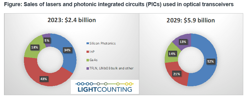
LightCounting: Silicon Photonics chip market to hit $3 billion in 2029
Light Counting on Silicon Photonics and Optical Switching at SC22
Synopsys and Juniper Networks form new company to pursue “open” silicon photonics platform
Technavio: Silicon Photonics market estimated to grow at ~25% CAGR from 2024-2028
The global silicon photonics market size is estimated to increase by $5.24 billion from 2024-2028, according to Technavio. The market is estimated to grow at a CAGR of almost 24.88% during the forecast period. Increasing need for higher bandwidth is driving market growth, with a trend towards emergence of optical data centers. However, lack of global standards and guidelines poses a challenge.
The decades old global Silicon Photonics market is now experiencing significant growth due to the increasing demand for high-speed data transfer in various industries. With Internet traffic from cloud computing, 5G technology, IoT, and AI-powered devices, there is a need for more efficient and low-power solutions.
Silicon photonics uses integrated circuits (ICs) for optical communications, thereby reducing power consumption compared to electronic technologies.
Key components of silicon photonics include transceivers, optical interconnects, lasers, modulators, and photodetectors. These are used in data centers, telecommunication networks, and interconnection networks. The market is also driven by the adoption of 5G network, self-driving cars, and high-speed kits for point-of-care testing and imaging data. Silicon photonics uses optical waveguides, optical modulators, and photodetectors made from silicon, silicon nitride, and other photonic components. These components are more compact and less susceptible to thermal effects compared to traditional fiber-optic solutions. Additionally, the use of high-powered laser sources, thermal stress management, and liquid-crystal cladding helps mitigate thermal effects and improve performance.

The market for silicon photonics is expected to grow in IT & telecommunications and consumer electronics sectors, with applications in broadband services, telecom service providers, and broadband connections. This growth is driven by the need for high-speed data transfer and low power consumption, making silicon photonics a promising solution for the future of optical communications and data storage systems.
Silicon photonics is now targeted at optical data centers, providing enhanced capabilities for data transmission, processing, and storage. By integrating high-speed, high-bandwidth optical interconnects directly onto silicon chips, silicon photonics enables seamless communication between different data center components. This results in faster data transfer rates, lower latency, and increased scalability, making it an ideal solution for modern applications like cloud computing, artificial intelligence, and big data analytics. The continuous growth in cloud-based applications and big data analytics has significantly expanded the scale of data center networks. Silicon photonics, with its advantages over traditional copper-based interconnects, is a crucial technology in addressing the demands for faster and more efficient data center infrastructure.
The communications industry’s growth is driving the demand for silicon photonics due to its ability to transmit wider bandwidth signals with low latency and maintain signal quality during long-distance communication with minimal loss. Silicon photonics is a key technology in optical communication systems, enabling the transfer of large amounts of data at high speeds. Increased bandwidth and low latency requirements have fueled the demand for silicon photonics-based devices such as receivers, transmitters, and modulators.
Communications Industry – Market size and forecast 2018 – 2028 (USD Mn):
The global silicon photonics market is experiencing significant growth due to increasing demand for high-speed data transfer in various industries. With the Internet traffic from cloud computing, 5G technology, IoT, and AI-powered devices, there is a need for more efficient and low-power optical communications solutions.
The proliferation of data centers and cloud computing infrastructure is a major factor driving the market’s growth. Vendors like Cisco Systems Inc. And Intel Corp. Offer silicon photonics solutions for high-speed data transmission in data center environments. The evolution of 5G networks is another significant factor, as silicon photonics supports 5G networks with low latency and high capacity at a low cost and power per bit. With the increasing investment in 5G networks, the demand for silicon photonics is also expected to rise, boosting the growth of the global silicon photonics market through the communications segment.
Silicon photonics vendors include: AIO Core Co. Ltd., ams OSRAM AG, Broadcom Inc., Corning Inc., Hamamatsu Photonics KK, II VI Inc., Infinera Corp., Innolume GmbH, Intel Corp., International Business Machines Corp., IPG Photonics Corp., MACOM Technology Solutions Inc., NKT Photonics AS, Nokia Corp., NVIDIA Corp., OpenLight Photonics Inc., OSCPS Motion Sensing Inc, RANVOUS Inc., Sicoya GmbH, TRUMPF SE Co. KG, and Cisco Systems Inc.
Market Challenges:
- Lack of global standards and guidelines
- Availability of substitute technologies for silicon photonics
- High heat generation by photonic components
Silicon photonics offers a promising solution with its integration of photonics and electronic components on a single silicon chip. However, challenges such as thermal effects, power consumption, and thermal stress in high-powered laser sources remain. Transceivers, optical interconnects, and lasers are key components in this market, along with modulators, photodetectors, and optical waveguides. Data centers, telecommunication, and IT and telecommunications are major end-users, with consumer electronics and automotive industries also adopting silicon photonics for high-speed kits in self-driving cars and point-of-care testing. Optical network infrastructure, including fiber-optic and active optical cables, is a significant application area. The market is expected to grow further with advancements in silicon nitride, optical multiplexers, attenuators, and other photonic components.
The absence of standardized protocols and specifications in the silicon photonics market poses challenges for both manufacturers and customers. Without universally accepted standards, the integration of silicon photonics components into existing optical communication systems and networks becomes complicated. Compatibility issues arise, product development and manufacturing processes are complicated, and implementation costs increase. Furthermore, the lack of clear standards results in inconsistent performance metrics, making it difficult for customers to compare and evaluate different silicon photonics solutions effectively. Standardization is crucial for the widespread adoption of new technologies, and its absence in the silicon photonics market hinders its growth and potential impact on the optical communication industry.
References:
LightCounting: Silicon Photonics chip market to hit $3 billion in 2029
Light Counting on Silicon Photonics and Optical Switching at SC22
Synopsys and Juniper Networks form new company to pursue “open” silicon photonics platform
LightCounting: Q1 2024 Optical Network Equipment market split between telecoms (-) and hyperscalers (+)
https://viodi.com/2013/11/08/silicon-photonics-cisco-intel-see-light-at-the-end-of-the-tunnel/
LightCounting: Silicon Photonics chip market to hit $3 billion in 2029
Light Counting on Silicon Photonics and Optical Switching at SC22
Silicon photonics continues to progress but is yet to be adopted for high-performance computing and server architectures, according to market research firm Light Counting.
However, the Super Compute 2022 (SC22) conference hosted two silicon photonics firsts:
- Professor Keren Bergman of Columbia University reported a working 5Tbit/s transmitter optical chiplet implemented using 80 channels and 3D packaging. The accompanying receiver chip is working and is being lab-tested.
- Ayar Labs demonstrated its 2Tbit/s TeraPHY chiplet in an end-to-end link, sending and receiving data.
During the panel discussion on high-performance computing and silicon photonics, Intel’s Fabrizio Petrini addressed head-on why optics had such a low profile at the show. “The reality is there is a lot of skepticism about this technology. The adoption is not going to happen anytime soon,” he said.
Systems designers don’t see the implications until they embrace this technology. But factors are aligning for change, and a transition point is being approached in how systems are built, he says; the implications for systems and disaggregation are enormous.
Optical switching is another technology that has been on the fringes of the market for decades. It was all the rage from 1998-2001, but then fizzled out as there weren’t any large scale commercial deployments of photonic switches.
LightCounting reported in August that Google had been using photonic circuit switching in its cloud resident data centers for several years. The 136×136 port optical circuit switch is Google’s own design.
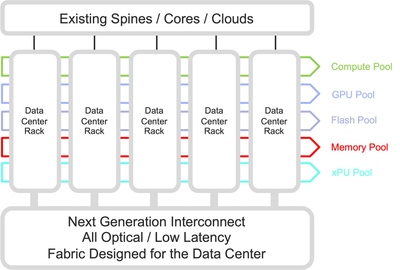
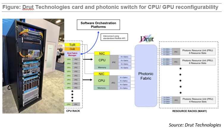
At SC22, a start-up, Drut Technologies, demonstrated its interface card working with a photonic switch at the top of a SuperMicro server rack. The system allows the server’s CPUs to dynamically configure the resources they need (memory, GPUs) tailored for workloads.
Synopsys and Juniper Networks form new company to pursue “open” silicon photonics platform
Synopsys Inc. and Juniper Networks announced that they have closed a transaction to form a new, separate company that will provide the industry with an open silicon photonics platform to address the growing photonic requirements in applications such as telecom, data communications, LiDAR, healthcare, HPC, AI, and optical computing. The new company’s open silicon photonics platform will include integrated lasers, optical amplifiers, and a full suite of photonic components to form a complete solution that will be accessible through a Process Design Kit (PDK). The platform will enable a new level of integration at an unmatched price point, with the lowest power consumption for high-performance Photonic Integrated Circuits (PICs). The name of the new company will be announced at a later date.
The terms of the agreement have not been disclosed at this time. The new company will be jointly owned by Synopsys and Juniper, with Synopsys as the majority owner. The new company’s results will be consolidated into Synopsys financials. While Synopsys expects the investment to be slightly dilutive to fiscal 2022 earnings, the investment is not material and will not affect Synopsys’ fiscal second quarter and full year 2022 guidance ranges provided on February 16, 2022. There is no change to Juniper’s full year financial outlook as a result of this transaction.
The new company is being formed, in part, from the carve-out of integrated silicon photonics assets from Juniper, which includes more than 200 patents on photonic device design and process integration. While part of Juniper, the new company has closely collaborated with Tower Semiconductor to develop and qualify Tower Semiconductor’s PH18DA process technology to enable the industry’s first “laser-on-a-chip” open silicon photonics platform. To demonstrate capabilities of this platform and accelerate customer adoption of the technology, the new company has created 400G and 800G photonics reference designs with integrated lasers and expects first samples to be available in summer 2022.
“Silicon photonics is a rapidly growing market that is transforming many industries and creating exciting opportunities for new applications in the future,” said Sassine Ghazi, president and chief operating officer at Synopsys. “The new company’s open silicon photonics platform, combined with Synopsys’ existing investment in a unified electronic photonic design automation solution consisting of OptoCompiler™, OptSim™, PrimeSim™, Photonic Device Compiler and IC Validator™ products, will help reshape the optical computing industry, enabling companies to cost-effectively shift to integrated lasers and significantly accelerate development of photonic IC designs.”
“This revolutionary technology will change the economics of how people are going to build photonic systems,” said Rami Rahim, CEO of Juniper Networks. “We have been strong supporters of integrated silicon photonics and we believe the new company will drive development of these systems by using an advanced open platform that will dramatically reduce costs and increase the performance and reliability of designs across multiple use cases. We are excited to continue to collaborate with the new company to enable a broad ecosystem to efficiently develop next-generation optical transceiver and co-packaged designs.”
A key challenge for silicon photonics has been the cost of adding discrete lasers, which includes the manufacturing as well as the assembly and alignment of those lasers onto the photonic chip. This becomes more important as the number of laser channels and the overall bandwidth increases. By processing the Indium Phosphide (InP) materials directly onto the silicon photonics wafer, the PH18DA platform reduces the cost and time of adding lasers, enabling volume scalability and improved power efficiency. In addition, monolithically integrated lasers on silicon wafers improves overall reliability and simplifies packaging. This “Laser-on-a-Chip” open silicon photonics platform will bring integrated photonics to a host of new applications and markets that were previously not thought possible. The first Multi-Project Wafer (MPW) is scheduled to be taped out in Q2 2022.
“We have had a long history of successful collaboration with Juniper Networks on integrated photonics. The new company formed by Synopsys and Juniper will strengthen and accelerate the adoption of the silicon photonics platform,” said Russell Ellwanger, CEO of Tower Semiconductor. “Providing an open silicon photonics platform consisting of integrated lasers that has been qualified on Tower’s process will enable customers to create innovative products with the potential to transform the industry.”

Editor’s Note:
Intel has been working on Silicon Photonics for almost two decades.
- In 2004, Intel scientists created the first transistor-like device able to encode data onto a light beam.
- In 2011, the company announced a 50 Gb/s silicon photonics link created by multiplexing four hybrid silicon lasers.
- In December 2021, the company launched a Research Center for Integrated Photonics for Data Center Interconnects. The center’s mission is to accelerate optical input/output (I/O) technology innovation in performance scaling and integration with a specific focus on photonics technology and devices, CMOS circuits and link architecture, and package integration and fiber coupling.
“At Intel Labs, we’re strong believers that no one organization can successfully turn all the requisite innovations into research reality. By collaborating with some of the top scientific minds from across the United States, Intel is opening the doors for the advancement of integrated photonics for the next generation of compute interconnect. We look forward to working closely with these researchers to explore how we can overcome impending performance barriers.” –James Jaussi, senior principal engineer and director of the PHY Research Lab in Intel Labs
Intel has recently demonstrated progress in critical technology building blocks for integrated photonics. Light generation, amplification, detection, modulation, CMOS interface circuits and package integration are essential to achieve the required performance to replace electrical as the primary high-bandwidth off-package interface.
Additionally, optical I/O has the potential to dramatically outperform electrical in the key performance metrics of reach, bandwidth density, power consumption and latency. Further innovations are necessary on several fronts to extend optical performance while lowering power and cost.
The Intel Research Center for Integrated Photonics for Data Center Interconnects brings together universities and world-renowned researchers to accelerate optical I/O technology innovation in performance scaling and integration. The research vision is to explore a technology scaling path that satisfies energy efficiency and bandwidth performance requirements for the next decade and beyond.
……………………………………………………………………………………………………………………………………………………………………………………………………………………………………………………………………………………..
About Synopsys:
Synopsys, Inc. is the Silicon to Software™ partner for innovative companies developing the electronic products and software applications we rely on every day. As an S&P 500 company, Synopsys has a long history of being a global leader in electronic design automation (EDA) and semiconductor IP and offers the industry’s broadest portfolio of application security testing tools and services. Whether you’re a system-on-chip (SoC) designer creating advanced semiconductors, or a software developer writing more secure, high-quality code, Synopsys has the solutions needed to deliver innovative products. Learn more at https://www.synopsys.com
About Juniper Networks:
Juniper Networks is dedicated to dramatically simplifying network operations and driving superior experiences for end users. Our solutions deliver industry-leading insight, automation, security, and AI to drive real business results. We believe that powering connections will bring us closer together while empowering us all to solve the world’s greatest challenges of well-being, sustainability, and equality. Additional information can be found at Juniper Networks (www.juniper.net) or connect with Juniper on Twitter, LinkedIn and Facebook.
Juniper Networks, the Juniper Networks logo, Juniper, Junos, and other trademarks listed here are registered trademarks of Juniper Networks, Inc. and/or its affiliates in the United States and other countries. Other names may be trademarks of their respective owners.
References:
Silicon Photonics – Cisco and Intel see “Light at the End of the Tunnel”