
Optical switching
PsiQuantum Targets AI Data Center Networks with Silicon-Photonic Optical Switching
Disclaimer: ChatGPT was used extensively for research contained in this article.
……………………………………………………………………………………………………………………………………..
Introduction:
As AI workloads expand and AI clusters grow, the networks connecting GPUs and other accelerators are becoming an increasingly important constraint on performance, power consumption and cost. Optical circuit switching (OCS) offers one way to improve connectivity by establishing direct optical paths between network ports without converting optical signals into electrical signals for packet-by-packet switching.
On October 28th, PsiQuantum [1.] unveiled an 8×8 optical circuit-switching demonstration built on its low-loss silicon-photonics platform, originally developed for quantum computing. The company reports promising laboratory results and is sharing demonstration samples with selected prospective customers. The key question is whether this technology can scale into a commercially competitive product for AI data centers.
Note 1. PsiQuantum was founded on the premise that photonic qubits, together with leverage of mature semiconductor manufacturing processes, would provide the fastest path to commercially useful, fault-tolerant quantum computers. Today, PsiQuantum builds tens of thousands of wafers of quantum chips in a tier-1 foundry, operates cryogenic cabinets supporting hundreds of chips, advances fault-tolerant algorithm development to solve critical problems across industries, and is developing a modular quantum computing platform designed to increase capability and scale. Each milestone brings us closer to delivering commercially useful quantum computing. The company’s headquarters is in Palo Alto, CA. Source: PsiQuantum
Optical Circuit Switching (OCS) for AI Data Centers:
Large AI clusters rely on high-speed interconnects to move model parameters, gradients, activations and other data among processors. Network congestion, communication overhead and power consumption can limit how effectively expensive accelerators are utilized. Ethernet and InfiniBand networks rely primarily on packet switches to route traffic dynamically.
OCS takes a different approach: it establishes direct optical connections between selected ports, allowing light to pass through the switching fabric without optical-electrical-optical conversion at the switch. This approach can complement conventional packet switching in AI clusters, particularly when communication patterns are predictable or recurring. A network controller can establish optical paths between selected racks or groups of accelerators, while packet switches handle traffic requiring flexible, fine-grained routing.
OCS is therefore a potential complement to conventional switching fabrics, not a wholesale replacement for Ethernet or InfiniBand. Its benefits depend on network architecture, traffic patterns, connection utilization and the overhead of reconfiguring optical paths.
Here’s an illustration of optical circuit switching in an AI data-center network. Optical circuit switches establish direct optical paths between selected network ports, complementing conventional packet switching. Conceptual illustration—not a depiction of PsiQuantum’s specific product or a verified implementation.
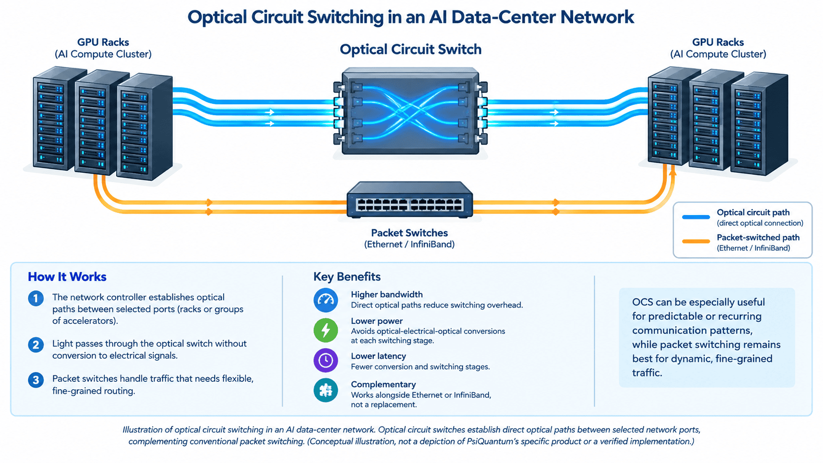
Image Credit: ChatGPT
………………………………………………………………………………………………………………………………………………………………………………………………………….
PsiQuantum’s 8×8 Demonstration:
PsiQuantum describes its first publicly disclosed device as a strictly non-blocking 8×8 switch, meaning any input can connect to any output. The silicon-photonic device operates without moving parts.
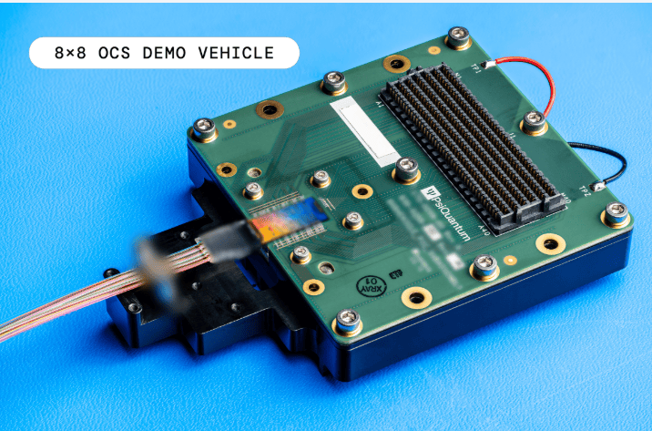
The company reports the following laboratory results:
| Parameter | Company-reported result |
|---|---|
| Switch configuration | 8×8 |
| Typical insertion loss | 1.2 dB |
| Crosstalk | 40 dB |
| Reconfiguration time | Less than 3 ms |
| Optical amplification | Not required |
Source: PsiQuantum, October 28, 2026. These are company-reported laboratory results, not independently verified benchmarks.
“This opportunity exists because we chose to solve the hardest scaling problems at the beginning of our roadmap to utility-scale quantum computing,” said Victor Peng, Chief Executive Officer of PsiQuantum. “As AI computing pushes infrastructure to its limits, we now have an opportunity to put our state-of-the-art technology to work today while continuing toward our ultimate goal: building and deploying the world’s first useful, fault-tolerant quantum computers.”
“AI is driving extraordinary growth in the scale and complexity of computing infrastructure, and optics will play an increasingly important role in enabling that growth,” said Rob Soderbery, Executive Vice President at PsiQuantum. “PsiQuantum has spent nearly a decade developing silicon photonics against some of the most demanding requirements imaginable. What we are demonstrating today is that this platform can deliver exceptional performance for optical circuit switching for AI computing.”
PsiQuantum has also developed barium titanate (BTO) integration at the 300mm wafer scale and uses a 64×64 BTO switch in its quantum systems. BTO is not required for the demonstration vehicle or initial products announced today, highlighting the performance of the underlying silicon photonics platform while preserving an additional path to faster, more advanced future products.
………………………………………………………………………………………………………………………………………………………………………………………………
EE Analysis:
Insertion loss measures the optical power lost as a signal passes through the switch. The reported 1.2 dB figure suggests that relatively little power is lost in the device itself.
Crosstalk measures unwanted signal leakage between channels, while reconfiguration time indicates how quickly the switch can establish a new connection arrangement.
A switching time below 3 milliseconds could support some scheduled or recurring AI communication patterns. However, suitability depends on workload characteristics, connection-management overhead and how effectively established paths are utilized.
PsiQuantum says its silicon-photonics platform leverages semiconductor manufacturing at Global Foundries in New York. It has also developed barium titanate integration at 300-mm wafer scale, but the company says this technology is not required for the demonstrated switch or its initial products. Its 8×8 device should therefore be judged on its own reported performance, rather than the potential capabilities of future products.
……………………………………………………………………………………………………………………………………………………………………………………………………………………………………………………………………..
Google Provides a Production-Scale Benchmark:
Optical circuit switching is already deployed in hyperscale data-center networks. Google’s Jupiter architecture provides an important real-world comparison.
In a 2022 ACM SIGCOMM paper, Google engineers described how Jupiter evolved from a conventional Clos network toward a direct-connect topology between aggregation blocks. Its Apollo optical circuit switches use micro-electromechanical systems (MEMS) mirrors to steer light between fiber ports. A software-defined networking (SDN) control plane dynamically adjusts the network’s logical topology and traffic paths, while packet switches continue to handle traffic routing.
Google’s paper reported that the broader evolution of Jupiter delivered a fivefold increase in network speed and capacity, a 30% reduction in capital expenditure and a 41% reduction in power consumption while serving live production traffic. These improvements resulted from the overall architecture—including optical switching, traffic engineering and network-management changes—not from the optical switches alone.
The distinction is important. Google has demonstrated production-scale OCS integrated with network control and traffic engineering. PsiQuantum has reported promising component-level results from an 8×8 silicon-photonic laboratory demonstration. The two systems also use different switching technologies.
Google’s experience nevertheless demonstrates that OCS can deliver substantial benefits when integrated into a carefully engineered network. PsiQuantum’s challenge is to show that its silicon-photonics approach can provide comparable practical value at scale.
The Commercial Test:
PsiQuantum must now demonstrate that its reported performance can be maintained in larger configurations and integrated into real AI data-center networks. The main questions are:
- Scalability: Can port counts increase without unacceptable optical losses, crosstalk, complexity or cost?
- Network integration: Can the switches work effectively alongside existing Ethernet and InfiniBand fabrics, with appropriate traffic scheduling and network management?
- Power and economics: Will the complete implementation reduce system-level power consumption or operating costs enough to justify adoption?
- Manufacturing and reliability: Can PsiQuantum deliver consistent production quality, operational reliability and competitive costs at the volumes data-center customers require?
The company says it plans to announce commercial products in the coming months. Larger configurations, independent performance measurements, customer trials and system-level demonstrations will be important milestones.
Lessons from the All-Optical Networking Hype Dictate Caution:
During the 1998–2001 telecom boom, all-optical networking was heavily promoted as the future of telecommunications, promising to eliminate electronic switching bottlenecks by keeping traffic optical throughout the network. Despite substantial investment and years of development, that broad vision never became the dominant commercial network architecture. NTT’s current IOWN and All-Photonics Network initiatives reflect renewed ambitions for end-to-end optical connectivity, but they do not erase the industry’s long history of overpromising.
This history warrants caution in evaluating PsiQuantum’s 8×8 demonstration. Optical circuit switching has proven useful in specific architectures, including Google’s production data-center network, but that does not establish a broad emerging market for every new OCS technology. PsiQuantum must demonstrate that its silicon-photonic approach can scale economically and deliver measurable system-level benefits in real AI data centers—not simply promising laboratory specifications.
Earlier all-optical-networking initiatives illustrate why attractive component specifications do not guarantee commercial adoption. However, OCS already has production deployments. The question here is whether PsiQuantum’s implementation offers a competitive advantage in a clearly defined deployment—not whether optical switching itself is viable.
Conclusions:
PsiQuantum’s 8×8 demonstration extends its silicon-photonics technology beyond quantum computing into a potentially valuable AI infrastructure market. Its reported insertion loss, crosstalk and sub-3-millisecond reconfiguration time warrant attention, but do not yet establish commercial scalability or an economic advantage over existing technologies.
Google’s Jupiter network shows that optical circuit switching can deliver benefits at hyperscale when combined with software-defined networking and traffic engineering. PsiQuantum must demonstrate that its distinct silicon-photonic approach can deliver similar practical value through larger switches, reliable integration and measurable system-level savings.
For AI data-center operators, the ultimate test is whether optical switching can deliver reliable, scalable and economically attractive connectivity that keeps expensive AI accelerators productively utilized.
The most informative next milestone would be a customer trial reporting port count, fiber-to-fiber loss, reconfiguration interruption, reliability, and workload-level performance and power against a specified baseline. Until then, PsiQuantum has presented a promising switching demonstration, not yet a demonstrated AI-networking advantage.
……………………………………………………………………………………………………………………………………………………………………………………………………..
References:
PsiQuantum, “Optical Circuit Switch.” https://www.psiquantum.com/optical-circuit-switch
PsiQuantum, “PsiQuantum Unveils Optical Circuit Switch Technology Built on Advanced, Low-Loss Silicon Photonics Platform,” October 28, 2026. https://www.businesswire.com/news/home/20261028890054/en/
Leon Poutievski et al., “Jupiter Evolving: Transforming Google’s Datacenter Network via Optical Circuit Switches and Software-Defined Networking,” ACM SIGCOMM 2022. https://doi.org/10.1145/3544216.3544265
Google Cloud, “The Evolution of Google’s Jupiter Data Center Network,” August 23, 2022. https://cloud.google.com/blog/topics/systems/the-evolution-of-googles-jupiter-data-center-network/
NTT’s IOWN is (finally) evolving to an All Photonics Network (APN); Physics based AI for enterprise OT
NTT’s IOWN provides ultra low latency and energy efficiency in Japan and Hong Kong
Oriole Networks photonic networking platform to be integrated with AMD GPUs/CPUs for next-gen AI data center fabrics
Technavio: Silicon Photonics market estimated to grow at ~25% CAGR from 2024-2028
LightCounting: Silicon Photonics chip market to hit $3 billion in 2029
Light Counting on Silicon Photonics and Optical Switching at SC22
Synopsys and Juniper Networks form new company to pursue “open” silicon photonics platform
Oriole Networks photonic networking platform to be integrated with AMD GPUs/CPUs for next-gen AI data center fabrics
London, England based Oriole Networks today announced continued progress in its collaboration with AMD in support of the UK’s Advanced Research & Invention Agency (ARIA) Scaling Inference Lab. The initiative integrates Oriole’s photonic interconnect architecture with AMD Instinct GPUs and AMD EPYC CPUs to evaluate next-generation data center fabrics capable of addressing the performance, latency, and energy constraints inherent in large-scale AI workloads.
The multi-year collaboration is advancing toward deployment of what is positioned as the first production-scale, all-photonic AI network fabric. The system is designed to deliver ultra-low latency and deterministic transport characteristics at the system level, leveraging optical circuit switching to optimize east-west traffic flows across accelerator clusters. The primary objective is to demonstrate how optical interconnect technologies can support large-scale inference and distributed AI processing under stringent performance and energy constraints.
Oriole’s PRISM photonic networking platform [2.] replaces conventional electronic switching in the network core with nanosecond-scale optical circuit switching. In contrast to packet-switched electronic fabrics, this approach is intended to reduce forwarding overhead, lower core power consumption, and improve end-to-end transport efficiency for accelerator-dense workloads. AMD is contributing compute hardware and technical collaboration to support modeling and execution of large-scale network workloads relevant to frontier AI systems. However, PRISM is not built for any single chip vendor. It works across any accelerator platform, giving the wider industry a path to frontier-scale system-wide performance without the need for proprietary stacks.
Note 1. Oriole Networks is a photonic networking company, developing disruptive technologies for AI/ML and HPC networking that will revolutionize data centers. These technologies address AI’s biggest challenges – speed, latency, and sustainability. Our holistic approach replaces energy-hungry electrical switching with photonic switching. By using only light to move data in the network, our solution will increase the efficiency of LLM training and inference to unprecedented levels while dramatically reducing the energy consumption of data centers, currently putting a huge strain on energy grids. We can offer faster, more efficient, and more sustainable AI without sacrificing the planet.
Note 2. Oriole’s PRISM is a fully photonic network system designed to provide port-level, all-to-all connectivity, eliminating the need for electrical switches and dramatically reducing the number of optical transceivers needed in the network. This evolution greatly reduces power consumption and latency, increases bandwidth, and strengthens network resilience by eliminating single points of failure.

Image Credit: Oriole Networks
…………………………………………………………………………………………………………………………………………………………………………………………………………………………………………..
The deployment also represents the first commercial implementation of Oriole’s technology following an R&D-to-production transition completed in approximately three years. The company states that its xPU-agnostic architecture is intended to support heterogeneous accelerator environments and broader industry rollout beginning in 2027.
Photonic networking architecture:
PRISM is designed to route data optically rather than electrically, using photonic circuit paths in place of conventional electronic switching elements. As AI training and inference workloads scale, data center interconnect requirements increasingly exceed the efficiency limits of traditional switch-based architectures, particularly in terms of power dissipation, thermal load, and communication latency.
By eliminating electronic switching in the fabric core, the PRISM architecture seeks to reduce core network power consumption and limit buffering- and queuing-related delay. The use of optical circuit switching is consistent with ongoing industry interest in photonic interconnects, co-packaged optics, and optical disaggregation as potential enablers of high-density AI clusters.
The company reports that the architecture can substantially reduce GPU idle time and improve system-level utilization by shortening data movement paths between compute nodes. It also indicates potential reductions in cooling demand and associated water usage due to lower network power dissipation.
Quotes:
James Regan, CEO of Oriole, said: “A year ago, we were proving the physics; today, we’re proving the business. Our collaboration with AMD has moved from concept to deployment to a system an order of magnitude larger, and the data proves this is already driving performance increases at pace. This is what it looks like when photonic networking stops being a research curiosity and starts being the foundation of how serious AI infrastructure gets built. There’s a big problem now with electrical switches, which are basically bottlenecking AI traffic, and it’s going to get worse. What we do is we replace all the electrical switches.”
“AMD is excited to collaborate with Oriole on the ARIA Scaling Inference Lab cluster,” said Madhu Rangarajan, corporate vice president, Compute and Enterprise AI business, AMD. “Oriole’s AI backend networking with nanosecond optical circuit switching represents a fundamentally different way to connect accelerators at scale. We are helping to validate how photonic fabrics can work alongside AMD compute to deliver the low-latency, high-bandwidth connectivity that AI Inference workloads demand.”
“Meeting the demands for modern AI requires rapidly identifying ways to improve the performance and cost-efficiency of large-scale AI clusters. ARIA is thrilled to collaborate with Oriole and AMD to demonstrate the benefits of this new technology and it’s exactly the type of collaboration, between innovative startups and industry leaders, that the Scaling Inference Lab was designed to foster,” said Suraj Bramhavar, Program Director at ARIA
Standards and interoperability context:
From a standards perspective, photonic AI fabrics remain an active area of industry development rather than a fully mature architectural class. Relevant technical domains include IEEE 802.3 optical Ethernet interfaces, ITU-T optical transport frameworks such as G.694 and G.709, and ecosystem work in optical interconnect and co-packaged optics initiatives.
A vendor-neutral, accelerator-agnostic photonic fabric may be of interest to standards and industry groups evaluating future data center interconnect models for AI and high-performance computing. The Oriole–AMD collaboration therefore provides an early reference point for assessing the operational characteristics, integration constraints, and interoperability implications of optical circuit-switched AI infrastructure.
……………………………………………………………………………………………………………………………………………………………………………………………………………………….
References:
Oriole to Deploy World’s First AI System with Pure Photonic Network to Supercharge Data Centers
https://www.fierce-network.com/cloud/oriole-networks-pushes-pure-photonic-networking-ai-data-centers
NTT’s IOWN is (finally) evolving to an All Photonics Network (APN); Physics based AI for enterprise OT
Goldman Sachs report: Optical Networking is the next mega trend in AI infrastructure
Hyperscaler design of networking equipment with ODM partners
Technavio: Silicon Photonics market estimated to grow at ~25% CAGR from 2024-2028
AT&T sets 1.6 Tbps long distance speed record on its white box based fiber optic network
AT&T claims it achieved a long distance world record top speed of 1.6Tb/s over a single wavelength across 296 km of its long haul fiber optic network (spanning Newark, New Jersey to Philadelphia, Pennsylvania). That is four times faster than its current top speed of 400Gb/s per wavelength!
The 1.6Tb/s wavelength carried two IEEE 802.3df-2024 standard-based 800 Gigabit Ethernet end-to-end circuits, an industry first. It is a full, uninterrupted data path utilizing a single light frequency across the entire fiber length between two endpoints. The single-carrier 1.6 Tb/s wavelength was transported alongside existing live customer traffic on 100Gb/s and 400Gb/s wavelengths.
Open-sourced white box switches were the network equipment used during the trial. The white boxes are designed using the Broadcom Jericho3 packet processor chip and can provide up to 18 x 800G network interface ports all within a 2RU platform. The (Israel based) DriveNets Network Cloud software-based solution is hardware-agnostic and runs open APIs on the white boxes to perform data and control plane functions, including routing at 800G. The use of white boxes and the disaggregation of the hardware and software control costs and facilitate faster innovation.
The two 800GbE signals from the white box were multiplexed to 1.6 Tb/s in Ciena’s WaveLogic 6 Extreme coherent optical transponder, which is the first coherent optical solution to use a 200Gbaud design and 3nm coherent DSP ASIC and to reach speeds up to 1.6 Tb/s on a single carrier. The WL6e technology reduces the space and power per transmitted bit by 50% compared to current 800G transponders. This trial is the first to demonstrate WL6e at 1.6Tb/s with standards compliant 800GbE clients.
In the Newark and Philadelphia offices, 800G DR8 pluggable transceivers from Coherent were installed in the white box router and WL6e transponder to create the cross-office connectivity between the packet and optical technologies. And 800GbE client signals, provided by Keysight’s AresOne-M 800GE testset, fed the white box through additional pairs of 800G DR8 pluggable client optics, allowing verification of end-to-end performance of the two 800GbE services from Newark to Philadelphia.
Quotes:
“Traffic on AT&T’s network continues to increase as consumers are using more connected devices,” said Mike Satterlee, vice president, Network Infrastructure and Services, AT&T. “We anticipate network traffic growth to double by 2028 and the technologies demonstrated in this trial will play a key role in AT&T’s continued efforts to keep up with increasing customer demand to send data, watch videos, and use streaming services.”
“This groundbreaking achievement with AT&T adds to a growing list of Ciena industry-firsts that push the boundaries of optical network speed and capacity,” said Dino DiPerna, senior vice president, Global Research and Development, Ciena. “Ciena’s WaveLogic 6 coherent optics will support AT&T’s next gen converged optical network and efforts to build a cloud-based and AI-ready network with greater scale, flexibility and efficiency.”

Verizon’s 1.6Tb/s on Metro Fiber Network:
AT&T’s announcement comes just a few months after arch-rival Verizon announced a 1.6 Tb/s milestone of its own. Verizon also, working with Ciena, achieved that peak speed on a single wavelength, but on its metro fiber (not long distance) network. Verizon is mainly looking to advance through M&A. Its proposed acquisition of Frontier Communications is still pending, with some Frontier shareholders insisting that the US$20 billion price tag undervalues the operator.
……………………………………………………………………………………………………………………………….
AT&T has spent the past six months demonstrating that it aims to build its way to fiber domination. It rolled out fiber to around 600,000 premises in the 4th quarter of last year, taking its total fiber footprint to 28.9 million locations; it is shooting for 50 million by the end of 2029.
References:
https://about.att.com/story/2025/data-transport.html
https://www.business.att.com/products/wavelength-services.html
https://www.telecoms.com/fibre/at-t-touts-1-6-tbps-fibre-speed-milestone-as-us-battle-continues
AT&T Highlights: 5G mid-band spectrum, AT&T Fiber, Gigapower joint venture with BlackRock/disaggregation traffic milestone
Nokia, Windstream Wholesale and Colt complete world’s first ultra-fast 800GbE optical and IP service trial
China Telecom with ZTE demo single-wavelength 1.2T bps hollow-core fiber transmission system over 100T bps
T-Mobile posts impressive wireless growth stats in 2Q-2024; fiber optic network acquisition binge to complement its FWA business
Bell Canada buying Ziply Fiber for C$7 billion; will become 3rd largest fiber ISP in U.S.
Light Counting on Silicon Photonics and Optical Switching at SC22
Silicon photonics continues to progress but is yet to be adopted for high-performance computing and server architectures, according to market research firm Light Counting.
However, the Super Compute 2022 (SC22) conference hosted two silicon photonics firsts:
- Professor Keren Bergman of Columbia University reported a working 5Tbit/s transmitter optical chiplet implemented using 80 channels and 3D packaging. The accompanying receiver chip is working and is being lab-tested.
- Ayar Labs demonstrated its 2Tbit/s TeraPHY chiplet in an end-to-end link, sending and receiving data.
During the panel discussion on high-performance computing and silicon photonics, Intel’s Fabrizio Petrini addressed head-on why optics had such a low profile at the show. “The reality is there is a lot of skepticism about this technology. The adoption is not going to happen anytime soon,” he said.
Systems designers don’t see the implications until they embrace this technology. But factors are aligning for change, and a transition point is being approached in how systems are built, he says; the implications for systems and disaggregation are enormous.
Optical switching is another technology that has been on the fringes of the market for decades. It was all the rage from 1998-2001, but then fizzled out as there weren’t any large scale commercial deployments of photonic switches.
LightCounting reported in August that Google had been using photonic circuit switching in its cloud resident data centers for several years. The 136×136 port optical circuit switch is Google’s own design.
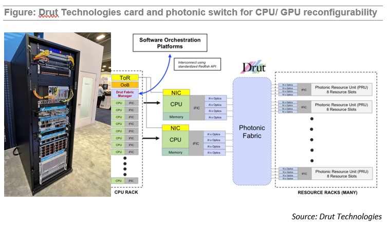
At SC22, a start-up, Drut Technologies, demonstrated its interface card working with a photonic switch at the top of a SuperMicro server rack. The system allows the server’s CPUs to dynamically configure the resources they need (memory, GPUs) tailored for workloads.