

Nvidia
AI-RAN Push: NVIDIA, Nokia, and Operators Drive Towards Distributed Compute Platforms
Introduction:
A massive industry consortium spearheaded by NVIDIA, Nokia, and leading global telecom operators has announced an expanded ecosystem initiative aimed at transforming traditional radio access network (RAN) sites into converged, distributed intelligence platforms. While vendor marketing frequently leans on the ambiguous hype of “AI-RAN,” this specific alignment underscores a tangible structural shift: the push to monetize edge network infrastructure by hosting centralized AI inference and processing workloads directly within the carrier’s decentralized footprint.
The coalition, which includes T-Mobile US, Deutsche Telekom, Orange, and SoftBank, is actively deploying multi-vendor frameworks to validate whether cell sites can simultaneously manage real-time layer-1/layer-2 radio scheduling and high-throughput external AI workloads on a single, unified hardware fabric.
Multi-Vendor Validation and Live Network Milestones:
Rather than remaining confined to isolated laboratory benchmarks, the initiative highlighted several live-network implementation milestones:
-
- T-Mobile US Commercial Network Execution: T-Mobile completed a live AI-RAN call within a commercial production environment, leveraging Nokia’s cloud-native RAN software integrated with NVIDIA’s accelerated computing architecture. The trial successfully demonstrated dynamic, real-time compute resource allocation between standard cellular traffic and concurrent AI applications.
- European Operator Deployment Frameworks: Deutsche Telekom and Orange are initiating deep architectural trials across their European footprints. These validation tests focus explicitly on multi-tenant control planes and the orchestration of heterogeneous GPU resources across legacy and greenfield environments.
- SoftBank Industrial Clusters: Moving past speculative trials, SoftBank is designing localized edge computing clusters that treat cell towers as distributed mini-data centers, targeted directly at hosting low-latency, localized autonomous vehicle and industrial robotics workloads.
Globally, nearly 20 telecom operators have publicly announced AI-RAN collaborations using Nokia anyRAN software and NVIDIA ARC.
- T-Mobile recently marked the world’s first AI-RAN call on its commercial network in Bellevue, Washington, running on commercial ARC servers, Nokia’s NVIDIA CUDA-accelerated RAN software and massive multiple-input multiple-output radios, and connected to an existing 5G Standalone core and a commercial smartphone.
- BT is planning live AI-RAN trials in Birmingham, England, with Nokia and NVIDIA in 2027.
- Deutsche Telekom has validated Nokia and NVIDIA’s commercial AI-RAN platform in Bonn and Oulu labs, including AI-enhanced uplink channel estimation to improve uplink user throughput, with plans to move to field trials in 2027.
- Elisa simultaneously ran voice, mobile data and video analytics on the NVIDIA ARC platform, marking a European first in Elisa’s over-the-air field environment using 5G spectrum. The trial clears the way for distributed deployment and commercial AI-RAN services in 2027.
- Orange is testing Nokia 5G software on NVIDIA ARC, focusing on AI-RAN spectral efficiency improvements and support for edge services in live networks.
NVIDIA is introducing two ARC configurations — MGX 2U and MGX 4U — designed for dense, high-capacity intelligence and radio workloads, typically deployed at centralized RAN sites. Powered by NVIDIA RTX PRO™ 6000 Blackwell Server Edition GPUs, the configurations will offer x86 and NVIDIA Vera CPU options. Dell Technologies, Quanta Cloud Technology and Supermicro will offer ARC-ready servers.
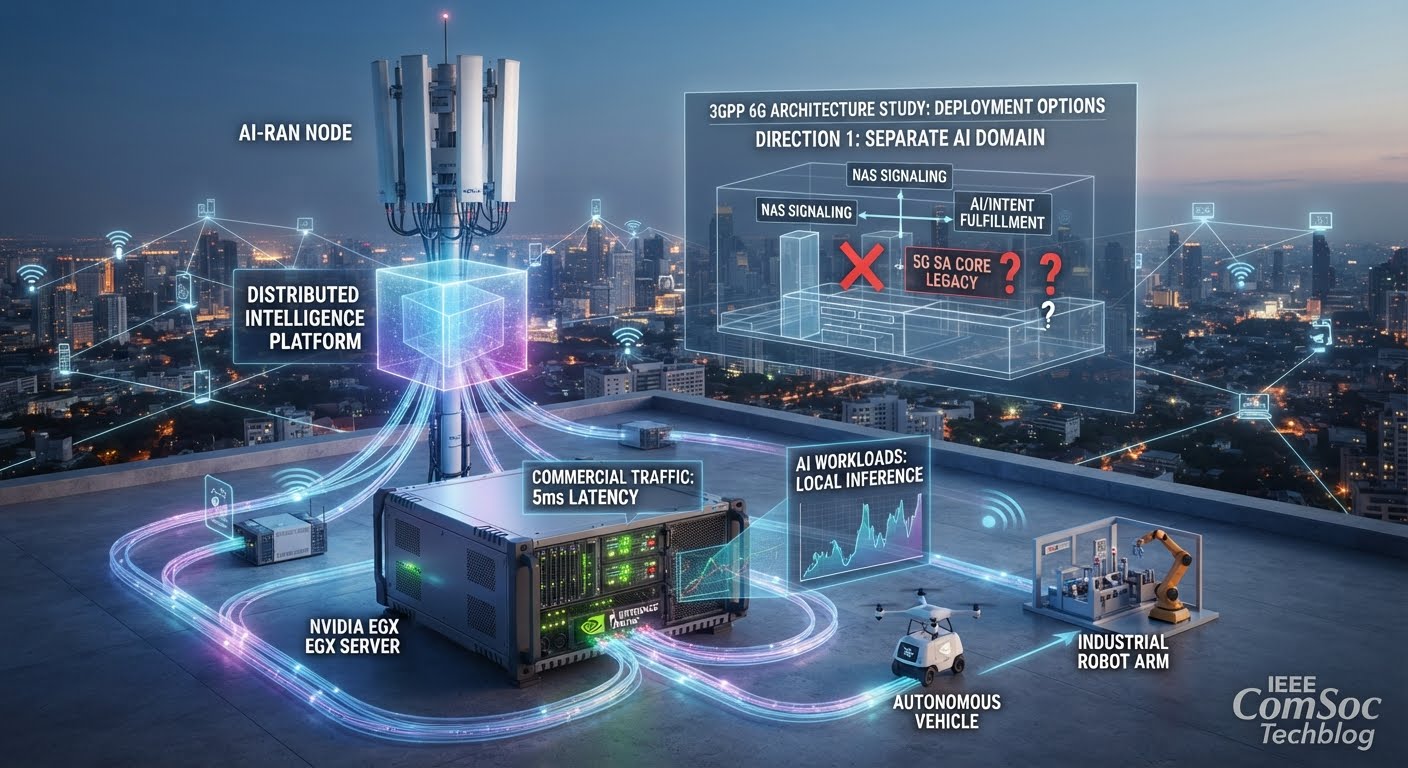
Image generated by Google Gemini
………………………………………………………………………………………………………………………………………………………………………………………
6G Splinter Risk – Will AI-RAN Interoperability Outpace the 6G SA Core?
This real-world push for decentralized AI-RAN execution exposes a critical timing and protocol gap within the broader standardization landscape. As vendors accelerate hardware deployments, the 3GPP SA2 Working Group remains technically fractured over how to formalize the underlying 6G core architecture. Rather than standardizing deterministic state behaviors, the current 6G study phase risks repeating the exact implementation voids that crippled 5G Standalone (SA) interoperability. Today’s commercial push for AI integration highlights the three architectural paths currently splintering 3GPP SA2:
-
- Direction 1 (Separate AI Domain): Anchors the core to the existing 5G Service-Based Architecture (SBA). It utilizes a dedicated AI domain for intent handling via the Service-Based Interface (SBI) while routing Non-Access Stratum (NAS) signaling through the AMF. Backed strongly by Western operators and vendors (including T-Mobile, Deutsche Telekom, Nokia, and NVIDIA), this path preserves 5G infrastructure investments but shifts the burden of multi-vendor integration directly to the device client.
- Direction 2 (AI Functionality in 6G NFs): Integrates machine learning natively within dedicated, standardized 6G network functions following legacy pipeline procedures.
- Direction 3 (Agent-Handled Connectivity): Eliminates traditional structural silos by deeply embedding autonomous AI agents directly into control and user plane procedures, bypassing the AMF entirely via a new Signaling Routing Function (SRF). This introduces massive procedural disruption to baseband silicon and core security frameworks.
………………………………………………………………………………………………………………………………………………………….
Conclusions – Bridging the Hype Gap:
The core engineering risk is that AI and machine learning models are fundamentally non-deterministic. If 3GPP restricts its focus to defining logical API endpoints rather than mandating strict behavioral state-machine realization, open agent-to-agent telemetry, and standardized model interchange formats, 6G will degenerate into a hyper-complex web of proprietary black boxes.
•Telcos have historically struggled to compete with hyperscalers (AWS, Azure, Google Cloud) on raw cloud storage and compute. AI-RAN could possibly the game because of physical close proximity and deterministic latency. By hosting AI workloads at the edge of the connectivity path, network operators might offer “Sovereign AI” and ultra-low-latency processing which centralized hyperscaler data centers physically cannot match.
As detailed in several previous IEEE Techblog posts (see References below), the telecom industry cannot afford another capital expenditure cycle driven by speculative lab benchmarks. By transforming cell towers into high-margin compute platforms, this distributed intelligence alliance offers carriers a concrete pathway to monetize low-latency edge workloads. However, for AI-RAN to achieve true multi-vendor utility, the engineering community must force 3GPP to bridge the gap between paper standards and deterministic software reality. We cannot afford to build another ghost in the machine.
………………………………………………………………………………………………………………………………………………………….
References:
6G Architecture and Economics: Core Network Evolution, AI Integration and Business Case
Warning: 6G core network must not repeat the 5G SA 3GPP architecture specs vs lack of interoperable standards
Sept 2026 3GPP meeting updates for 5G Advanced and 6G planning (with timeline for submisson to ITU-R WP 5D via ATIS)
Roles of 3GPP and ITU-R WP 5D in the IMT 2030/6G standards process
3GPP approves timelines for Release 21 which will specify 6G RAN, Core and 5G Advanced
Dell’Oro: RAN Market Stabilized in 2025 with 1% CAG forecast over next 5 years; Opinion on AI RAN, 5G Advanced, 6G RAN/Core risks
Ericsson leads SK Telecom AI RAN vs. NVIDIA’s GPU centric AI RAN Alliance
Ericsson goes with custom silicon (rather than Nvidia GPUs) for AI RAN
Dell’Oro: AI RAN revenue forecast: $35B from 2026-to-2030; 3 types of AI RAN explained
2026 OCP Summit: Full-Stack AI Networking Silicon from Nvidia/Cisco and Broadcom; Ethernet vs InfiniBand Interconnects
Executive Summary:
At the 2026 Open Compute Project (OCP) Global Summit in San Jose, CA this week, the multi-vendor push for open, gigawatt-scale AI networks reached a critical tipping point as Cisco and Broadcom deployed massive 102.4 Tbps Ethernet fabrics to challenge Nvidia’s proprietary grip. These and other networking silicon companies are responding to what Cisco executives call a new “Network Supercycle” triggered by agentic AI workloads. The architectural battle lines for gigawatt-scale AI infrastructure were drawn between open ecosystems and proprietary stacks. Broadcom championed the open alternative by introducing its 102.4 Tbps Tomahawk 6 switching platform and third-generation TH6-Davisson Co-Packaged Optics (CPO) to drastically reduce power consumption across clusters exceeding 100,000 accelerators.
- Cisco accelerated this so called “Network Supercycle” by highlighting massive hyperscaler traction for its custom Silicon One P200 routing chips, which Microsoft and Alibaba Cloud have integrated into their custom architectures to handle dense, geographically distributed AI workloads.
- Nvidia defended its market dominance with its Quantum-3 InfiniBand switches and native sub-2µs point-to-point latency; however, despite InfiniBand technically originating as an open industry standard, Nvidia’s sole manufacturing monopoly, closed software integration with CUDA, and proprietary extensions like SHARP have effectively turned it into a vertically locked, high-premium ecosystem. This strict architectural division has forced hyperscalers to choose between the seamless, turnkey acceleration of Nvidia’s proprietary pipeline for tight scale-up GPU environments, or the superior multi-vendor economics, flexibility, and anti-lock-in guardrails offered by Broadcom and Cisco’s open Ethernet frameworks.
- Broadcom launched an open Ethernet fabric architecture designed for gigawatt-scale clusters scaling past 100,000 parallel AI accelerators, showcasing innovations like the 102.4 Tbps Tomahawk 6 and Jericho 4 silicon. The company also introduced TH6-Davisson Co-Packaged Optics, Thor Ultra 800G NICs, and Open Rack Version 3 blueprints to compete with proprietary InfiniBand stacks. You can read more about Broadcom’s announcements at the official corporate site.
I. Cisco has worked with Nvidia on an Ultra-Dense Small Form-Factor Pluggable (USFP), a transceiver that conforms to the Octal Small Form-Factor Pluggable (OSFP) footprint that governs most high-speed datacenter transceivers today. Cisco said USFP enables the industry to accelerate AI by building on the ecosystem models that have powered today’s AI networks. By combining a path to higher-capacity fabrics and improved efficiency with familiar operational practices, USFP helps customers scale AI infrastructure while maintaining the flexibility, interoperability, and consistency required at scale.
Unlike other optical transceivers, the leading versions of which are designed to handle 200-Gb/s today, USFP provides 400-Gb/s full-duplex data rates over 16 lanes with 32 in the future, achieving transmission rates from 6.4 Tb/s up to 12.8 Tb/s. Nvidia said scalability is facilitated by an internal connector technology that reduces wear and improves signal integrity. USFP works with switches and SmartNICs. The new USFP is designed to save power without requiring liquid cooling, something that other solutions feature—most notably Arista Network’s eXtra-dense Pluggable Optics (XPO) solution, which packs its own liquid-cooled cold plate.
Cisco and NVIDIA claim that, compared to an OSFP module supporting 200-Gb/s, the new USFP has approximately 1.3X the power efficiency. At the same time, the USFP matches the footprint of today’s OSFP transceivers, making for an easier transition than the new form-factor XPO, which Arista says improves density by a factor of 4X. The two companies said they’ll work with a “community-led multi-source project” to create an open industry specification for USFP. Members of that “community” were not identified. 
Source: NVIDIA and Cisco
In a blogpost, Cisco executives Bill Gartner, SVP and GM, Optical Systems and Optics, and Will Eatherton, SVP Networking Engineering, stated:
“To help customers scale AI infrastructure efficiently and sustainably, Cisco takes a full-stack, co-designed platform approach that combines silicon, high-density systems, optics, software, and operational expertise. USFP reflects that philosophy. Rather than a standalone innovation, it is part of a broader platform vision that advances scale, efficiency, and performance while preserving the deployment, serviceability, and lifecycle models customers depend on.”
………………………………………………………………………………………………………………………………………………………………………
Cisco also highlighted massive cloud traction for its custom Silicon One P200 routing chip, which provides 51.2 Tb/s of high-buffering switching capacity designed to seamlessly link vast, geographically distributed AI data sites. Microsoft and Alibaba Cloud.
“As our infrastructure demands grow, the P200’s robust architecture provides the speed and enhanced buffering capabilities necessary to address the increasing scale of our cloud and high-performance services,” said Anand Ramakrishna, Corporate Vice President, Engineering, Microsoft, in a statement.
Alibaba has embedded the Silicon One P200 into its Quantum Cat router. “We paired Cisco’s silicon with Alibaba’s custom systems and the SONiC operating system,” stated Dennis Cai, Vice President, Head of Network Infrastructure, Alibaba Cloud Intelligence Group. “This combination … delivers the flexibility and operational power required for some of the world’s most demanding networks.”
Cisco also said that its previously announced 102.4-Tb/s Silicon One G300 is now available for customer sampling, with some G300-powered systems shipping to customers. Another chip, the 51.2-Gb/s G302, is designed to function at top-of-rack (ToR) deployments for scale up or scale across infrastructure.
Cisco’s OCP announcements indicate the networking market leader’s efforts to continue unifying its full-stack strategy around its own silicon, switching, and software, a tack that so far has proved successful.
………………………………………………………………………………………………………………………………………………………………………
-
- Tomahawk 6 & Jericho 4 Silicon: Broadcom demonstrated live partner systems running its 102.4 Tbps Tomahawk 6 switching platform for low-latency frontend fabrics, alongside Jericho 4 silicon for deep-buffered scale-out routing.
- TH6-Davisson Co-Packaged Optics (CPO): This third-generation CPO architecture integrates optics directly onto the switch substrate. By eliminating internal copper traces to traditional transceivers, it drastically reduces power consumption per gigabit.
- Thor Ultra 800G NICs: These high-performance network interface cards support line-rate 800 Gbps RoCE (RDMA over Converged Ethernet) throughput, accelerating memory-to-memory data transfers while bypassing CPU overhead.
- ORV3 Ecosystem Blueprint: Broadcom aligned its PCIe Gen 6 switches, retimers, and optical components with the Open Rack Version 3 (ORV3) and Open Rack Wide standards, supporting dense liquid-cooled rack configurations.
- Open Standard Commitments: Under standardizing frameworks like ESUN (Ethernet for Scale-Up Networking), Broadcom pitched open Ethernet as the primary economic and physical alternative to proprietary InfiniBand fabrics for frontier AI clusters.
- Enterprise LAN and Client-to-Server Interconnects: Connects standard server racks to local networks, user devices, and the broader internet.
- Front-End Data Center Networks: Manages standard cloud computing workloads, database queries, and multi-tenant hosting environments.
- Emerging AI Backends (via RoCEv2): Through frameworks like the Ultra Ethernet Consortium (UEC) and platforms like NVIDIA’s Spectrum-X, modern 800Gbps Ethernet is increasingly deployed by hyperscalers (such as Meta and xAI) for AI clusters due to its superior Total Cost of Ownership (TCO) and rapid innovation cycle.
- Ecosystem and TCO: Leverages a massive global supply chain and existing IT skills, avoiding the proprietary premium and single-vendor lock-in common with InfiniBand.
- RoCE Adaptability: Uses RDMA over Converged Ethernet (RoCEv2) along with Priority Flow Control (PFC) to emulate the low-latency, lossless advantages of InfiniBand over traditional network lines.
-
- Header Optimization: Standard Ethernet headers carry massive protocol overhead that increases latency for small data frames. ESUN implements a streamlined, compact 4-byte ESUN Header (EH) to maximize packet efficiency, strip away unneeded bytes, and drastically lower transport latency.
- Lossless Reliability & Tail Latency Control: AI workloads depend heavily on synchronized “collective” mathematical operations where a single dropped packet can stall the entire training run. ESUN implements advanced Credit-Based Flow-Control (CBFC) to guarantee zero packet loss and tightly manage jitter and tail latency.
- Decoupled Multi-Vendor Interoperability: ESUN focuses strictly on how network switches and network interface cards (NICs) handle frame formatting and packet switching. By keeping the fabric protocol-agnostic, it allows accelerators to define their own host-side transport layers independently, allowing operators to mix-and-match silicon suppliers.
| Networking Initiative | Governing Body | Primary Focus | Role in the AI Ecosystem |
|---|---|---|---|
| ESUN | Open Compute Project (OCP) | Scale-Up Network Fabric (L2/L3 switching and framing) | Optimizes the actual network switches and packet formatting inside the physical rack. |
| SUE-T (Scale-Up Ethernet Transport) | Open Compute Project (OCP) | Scale-Up Endpoint Transport (XPU-to-XPU communication) | A specialized transport protocol layer designed to work natively inside the ESUN switch framework to handle load balancing and transaction scheduling. |
| UEC (Ultra Ethernet Consortium) | Linux Foundation | Data Center-Wide Networks (Initially Scale-Out, expanding to Scale-Up) | A broader, top-to-bottom architecture that ESUN actively pulls specifications and best practices from to align with global standards. |
III. Ethernet vs. InfiniBand for Interconnects:
The structural battle between Broadcom’s open Ethernet platform and Nvidia’s proprietary InfiniBand fabric [1.] are direct competitors for backend compute & storage interconnects in data centers, high-performance computing (HPC), and AI clusters within data centers. The technical architectures, advantages, and philosophies of both approaches contrast sharply.
Note 1. InfiniBand by itself is an open, industry-standard specification managed by the InfiniBand Trade Association (IBTA). Nvidia acquired its primary architect, the Israeli company Mellanox, for $6.9 billion in 2019. However, in the context of modern AI data centers, Nvidia has effectively turned InfiniBand into a de facto proprietary ecosystem through vendor monopoly and closed optimizations. Here’s how that happened:
-
- Vendor Monopoly: Nvidia is the sole manufacturer of AI-class InfiniBand silicon. Competitors like Intel abandoned the technology, while Broadcom and Cisco focus entirely on Ethernet.
- Proprietary Extensions: Nvidia injects closed-source hardware features like SHARP (which offloads AI math directly onto switches) that require a strict end-to-end Nvidia hardware pipeline.
- Software Lock-In: Management and orchestration tools are tightly bound to Nvidia’s proprietary CUDA and Unified Fabric Manager (UFM) stacks.
| Aspect | The Theoretical Standard | The Modern AI Reality |
|---|---|---|
| The Spec | Open, industry-standard managed by the IBTA. | Monopolized by a single vendor (Nvidia). |
| The Silicon | Anyone can build an InfiniBand chip. | Nvidia is the sole manufacturer of AI-class InfiniBand. |
| The Interconnect | Interoperable with various hardware platforms. | Tightly coupled with Nvidia GPUs and CUDA via proprietary extensions like SHARP. |
| Feature / Metric | Broadcom Open Ethernet Platform | Nvidia Proprietary InfiniBand Fabric |
|---|---|---|
| Architectural Philosophy | Open ecosystem. Decouples compute from networking to prevent vendor lock-in. | Vertically integrated. Tightly couples GPUs, switches, and software for a turn-key solution. |
| Top Raw Bandwidth | 102.4 Tbps single-chip switching capacity via Tomahawk 6. Supports native 800G per port. | 51.2 Tbps single-chip switching capacity on the latest Quantum-3 switches (400G per port). |
| Latency Profile | Average < 5µs using RoCE v2. Drops significantly via UEC 1.1 optimizations. | Native sub-2µs point-to-point latency with near-zero jitter. |
| Congestion & Reliability | Uses packet spraying, adaptive routing, and link-level retries via Ultra Ethernet Consortium (UEC). | Native credit-based flow control. Prevents buffer overflows at the hardware level for a completely lossless fabric. |
| Optical Integration | Leading the industry with Co-Packaged Optics (CPO) integrated onto the switch substrate. | Moving toward CPO integration in upcoming H2 2026 platform refreshes. |
| Relative Costs | Standard commoditized pricing. Roughly 1/3 the hardware cost of InfiniBand. | Premium pricing tied directly to Nvidia’s exclusive compute bundle. |
…………………………………………………………………………………………………………………………………………………………………………………………………………………………………………
References:
https://www.futuriom.com/articles/news/cisco-shows-full-stack-networking-strategy-at-ocp/2026/10
https://blogs.cisco.com/news/cisco-and-nvidia-announce-usfp-expanding-the-path-to-ai-connectivity
https://www.broadcom.com/company/news/resources/media-kits/2026-ocp-global-summit
Cisco Execs: New “Network Supercycle” as Agentic AI Workloads Reshape Telecom Infrastructure
Cisco’s Silicon One G300 as the dominant AI networking fabric, competing with Broadcom’s Tomahawk 6 series
Analysis: Ethernet gains on InfiniBand in data center connectivity market; White Box/ODM vendors top choice for AI hyperscalers
Networking chips and modules for AI data centers: Infiniband, Ultra Ethernet, Optical Connections
Will AI clusters be interconnected via Infiniband or Ethernet: NVIDIA doesn’t care, but Broadcom sure does!
The AI Infrastructure Build-Out: A $10 Trillion Bet on Compute, Power, and Networks
Huawei’s Ascend Silicon Roadmap Extends From AI Chips to Cluster-Scale Infrastructure
Google’s TPU Business Outpaces Rivals as Hyperscalers Accelerate Custom AI Silicon Strategies
Meta’s “Iris” AI Chip for MTIA: Implications for Telecom-Grade Optical Networking, DCI and High Capacity Ethernet Fabrics
Analysis: Nvidia–MediaTek Deepen AI Platform Collaboration -What it Means for AI RAN & DCI
Executive Summary:
Nvidia has expanded its partnership with Taiwan based semiconductor firm MediaTek, committing $3.5 billion to a bond investment the two companies describe as a deepening of their “longstanding collaboration to build the next generations of AI computing platforms.” The move extends Nvidia’s pattern of strategic capital deployment across its compute ecosystem, this time reaching into custom silicon and advanced packaging.
According to the announcement, the collaboration couples Nvidia’s accelerated computing, AI, graphics, and software stack with MediaTek’s capabilities in custom silicon, high-performance computing (HPC), system-on-chip (SoC) design, and advanced packaging. MediaTek vice chairman and CEO Rick Tsai framed the investment as reinforcing a relationship spanning “cloud AI infrastructure, local AI computing and automotive in the era of physical AI,” combining Nvidia’s accelerated-computing and AI software ecosystem with MediaTek’s AI technology portfolio and custom-silicon resources.
Over the past several years, MediaTek has repositioned itself from a supplier of predominantly mid- and low-tier handset chipsets into a presence across smartphones, AI data centers, automotive, and IoT. Securities firm Yuanta Financial Holdings expects the closer alignment to accelerate MediaTek’s transition from edge AI into data-center infrastructure, device-based AI computing, and automotive platforms. Trading in MediaTek shares was suspended on the Taipei exchange Tuesday after the stock hit its daily 10% upside limit. The shares closed at NT$4,315 (about US$136.05), reflecting investor enthusiasm for the deepening of the collaboration.
NVIDIA and MediaTek are collaborating in three major areas:
- AI infrastructure: MediaTek will work with NVIDIA’s NVLink Fusion ecosystem to enable customers to develop custom AI infrastructure designed to integrate with NVIDIA rack-scale systems and AI factories.
- Local AI computing: The companies will continue to collaborate on multiple generations of NVIDIA RTX Spark™ and DGX Spark™ PC chips, powering consumer PCs, AI developer supercomputers and enterprise-class workstations, that integrate NVIDIA GPUs with MediaTek SoCs.
- Automotive: MediaTek and NVIDIA will continue developing platforms for AI-powered, software-defined vehicles in the era of physical AI.
“AI is transforming every computing platform — from the world’s largest AI factories to the PC and the car,” said Jensen Huang, founder and CEO of NVIDIA. “MediaTek is one of the world’s great semiconductor companies, with exceptional expertise in system-on-chip design, connectivity, leading performance and power efficiency. Together, we’re building platforms that bring NVIDIA accelerated computing to new markets and give customers the freedom to create differentiated AI systems at enormous scale.”
“MediaTek and NVIDIA share a vision for making advanced AI computing pervasive across the technology landscape,” said Rick Tsai, vice chairman and CEO of MediaTek. “NVIDIA’s investment strengthens a collaboration that spans cloud AI infrastructure, local AI computing and automotive in the era of physical AI. By combining NVIDIA’s leadership in accelerated computing and AI software ecosystem with MediaTek’s expertise in a diverse AI technology portfolio from edge to cloud, and our leadership position in custom silicon, we can accelerate innovation for our customers.”
Custom AI Infrastructure and NVLink Fusion:
Yuanta identified MediaTek’s participation in Nvidia’s NVLink Fusion as the most consequential element of the arrangement. Through that linkage, MediaTek could support the design of custom AI chips for clients while connecting them directly into Nvidia’s AI infrastructure — a complementary rather than competing role alongside the GPU vendor’s proprietary interconnect fabric.
The scale of the bond purchase also signals Nvidia’s long-term commitment to the relationship. Nvidia, currently the world’s most valuable company at roughly a $5 trillion market capitalization, has been deploying capital aggressively across both upstream and downstream partners. This latest deal, however, inevitably risks overlapping with other Nvidia investments — notably its $2 billion partnership with Marvell, which is also heavily oriented around NVLink Fusion and pitch-for the RAN with a one-chip architecture.
NVLink Fusion vs. Ethernet Scale-Out Interconnect:
NVLink Fusion and Ethernet-based scale-out interconnects target fundamentally different layers of the AI fabric, and the distinction turns on memory semantics rather than raw link rate. NVLink Fusion sits in the scale-up domain: it delivers memory-coherent, tightly coupled attachment for custom XPUs into Nvidia’s rack-scale NVLink fabric, with point-to-point GPU/XPU-to-GPU/XPU connectivity and an integrated high-bandwidth-memory interface (NVHBM) that trades die area and power for latency and bandwidth. It is proprietary, closed, and full-coherency by design — precisely the properties that make it hard for open standards to clone. Ethernet scale-out, by contrast, is the scale-out workhorse governing traffic between racks, pods, and clusters; it is loss-based, coarser-grained, and standardized through Ultra Ethernet and the broader IEEE 802.3 ecosystem.
The real contest is not NVLink against Ethernet so much as how much of the memory-coherent scale-up domain Ethernet-based challengers can capture. Standards-backed alternatives — UALink 2.0, Ultra Ethernet, and Broadcom’s Scale-Up Ethernet (SUE) — are pressing into scale-up territory, but they lack NVLink’s memory coherency and direct XPU-to-XPU connectivity, and SUE explicitly does not wire GPUs directly to GPUs. Meanwhile Nvidia’s strategy with NVLink Fusion is to co-opt custom XPUs (AWS Trainium4, and now MediaTek- and Marvell-designed silicon) into its fabric rather than let them migrate to those open scale-up paths. The practical outcome in the data center is a layered model — Ethernet surging in scale-out, and NVLink Fusion consolidating the latency-sensitive, memory-coherent scale-up spine — with Nvidia working to keep its proprietary layer the mandatory gateway that custom accelerators must pass through to reach the wider Ethernet-based world.
The $3.5 billion convertible-bond investment is best read not as a portfolio decision but as a defensive move within the AI rack-scale interconnect stack. The technical centerpiece is MediaTek’s adoption of the NVLink Fusion platform. Nvidia positions it as the connectivity technology and intellectual property that lets hyperscalers and AI-native operators drop custom accelerators (“XPUs”) and CPUs directly into its NVLink scale-up fabric.
MediaTek will now build against the three subsystems that define NVLink Fusion: the NVLink Fusion chiplet, which bridges a customer’s custom XPU to the NVLink scale-up domain over photonic or electrical interconnects (the chiplet itself carries up to ~1.8 TB/s of bidirectional bandwidth); NVLink-C2C, the high-bandwidth die-to-die link between XPUs, Nvidia’s Vera/Rosa CPUs, and other compatible processors; and NVHBM, a customized high-bandwidth-memory interface that trades off die area and power efficiency. The strategic significance is that Nvidia is effectively licensing its interconnect and memory layer as a licensable subsystem rather than enforcing a closed, all-Nvidia island — which lets it absorb “frenemy” silicon into the fabric instead of fighting it.
Two implications stand out for interconnect strategy:
-
A hedge on hyperscaler in-house silicon. AWS has already integrated its Trainium4 custom ASICs with NVLink Fusion for rack-scale deployment, and Google, Meta, Microsoft, and OpenAI are all advancing private accelerators. By standardizing the interface (NVLink Fusion, NVLink-C2C, NVHBM, chiplets, and rack-scale integration) that these custom XPUs must speak, Nvidia keeps chiplets, packages, memory, and racks—the connective infrastructure itself—inside its own revenue funnel. MediaTek, in turn, becomes the design conduit that helps hyperscalers and frontier model firms get to that tape-out without building an independent scale-up stack.
-
The scale-up vs. scale-out contest sharpens. NVLink remains essentially the only mature, memory-coherent scale-up fabric in production, whereas Ethernet is consolidating its dominance in scale-out (front-end and increasingly AI back-end) fabrics, and standards like Ultra Ethernet, UALink, and Broadcom’s Scale-Up Ethernet (SUE) are pressing into the scale-up domain. UALink and SUE, notably, lack NVLink’s memory coherency and point-to-point GPU-to-GPU connectivity, so NVLink Fusion’s positioning — co-opting custom XPUs rather than competing with them — lowers the attack surface those open standards could otherwise exploit.
The buy-in therefore consolidates Nvidia’s grip on the two layers that are hardest to commoditize: the latency-sensitive scale-up interconnect and the custom-silicon design flow that feeds it. What operators and chip partners give up is architectural independence — the bond structure and NVLink Fusion licensing effectively bind MediaTek into Nvidia’s ecosystem rather than allowing it to become an independent AI data-center silicon house.
What It Means for AI-RAN:
For the RAN, this is arguably a more consequential signal than the data-center economics. Nvidia’s AI-RAN play, via the AI Aerial software-defined accelerated-computing platform and its founding role in the AI-RAN Alliance, is built on having vRAN and AI workloads share the same GPU-accelerated infrastructure — what the community variously calls “AI for RAN,” “AI on RAN,” and “AI-and-RAN” on common hardware.nvidia+1
Here the MediaTek deal intersects directly with Nvidia’s earlier $2 billion Marvell partnership, which last year wired Marvell into the same NVLink Fusion platform for both the AI factory and AI-RAN ecosystem — Marvell supplying custom XPUs and NVLink Fusion-compatible scale-up networking, while Nvidia contributes the Vera CPU, ConnectX NICs, BlueField DPUs, Spectrum-X switches, and the rack-scale AI compute. The two arrangements are complementary in practice but overlapping in intent: Marvell owns the scale-up networking and the “one-chip-to-rule-the-RAN” custom silicon angle, while MediaTek brings SoC design, advanced packaging, and stronger reach into edge, automotive, and device-grade silicon. Together they give Nvidia two design houses capable of producing custom XPUs that plug into both data-center racks and AI-RAN infrastructure.
The operative question for IEEE readers is whether this broadens the AI-RAN supplier base going forward. Ericsson and Samsung have indicated their vRAN software built for Intel could be ported to AMD or Arm silicon with relatively modest effort, and Dell’Oro projections already have AI-RAN taking a significant share of the broader RAN market. Nvidia’s strategy is to ensure that, however the RAN silicon shakes out, the scale-up fabric and the custom-XPU design path remain NVLink Fusion-based — extending its data-center interconnect franchise into the radio access domain itself. The risk, flagged in the news report, is over-concentration: stacking Marvell and MediaTek onto the same NVLink Fusion foundation concentrates architectural leverage in Nvidia’s hands and could crowd out the open, multi-vendor fabric choices that O-RAN advocates would prefer to see served by standard Ethernet and UALink-style paths.
References:
https://www.lightreading.com/finance/nvidia-tips-3-5b-into-mediatek-in-latest-tech-partnership
Analysis: Nvidia’s $2 billion investment in Marvell; NVLink Fusion ecosystem & RAN vendor silicon strategy
Ericsson and MediaTek Demonstrate 3GPP-Based GNSS RTK Positioning with Sub-30cm Accuracy Over a Commercial 5G Network
5G infrastructure moves from coverage and speeds to cloud-native, orchestration, automation and AI-assisted networks
MediaTek overtakes Qualcomm in 5G smartphone chip market
Huge Risks for the proposed $500B AI Investments from Giant Wall Street firms
Disclaimer: Perplexity.ai was used for research and analysis in this article.
……………………………………………………………………………………………………………………..
Executive Summary:
This past Monday, six giant Wall Street asset managers, private-equity firms and banks announced an effort to raise $500 billion to keep fueling the A.I. boom by financing more data centers, power plants and chips. The proposed platform would direct capital to Nvidia customers—including AI startups and data-center operators—at precisely the point when many have struggled to obtain funding through ordinary credit channels.
We take that as a huge warning sign for the proposed AI investments. Here’s why: If the underlying projects offered clearly proven cash flows, predictable utilization and collateral with durable value, lenders would not need a specially assembled consortium, headline-scale commitments and Nvidia’s direct involvement to make the loans happen. The initiative appears designed to overcome a financing bottleneck created by the extraordinary gap between AI infrastructure spending and demonstrated AI revenue.
This proposed $500 billion AI-financing initiative is less a validation of durable AI economics than an admission that the sector’s spending plans have outgrown its customers’ ability—or willingness—to finance them conventionally. Rather than demonstrating independently sustainable demand, the arrangement risks extending an investment cycle increasingly dependent on vendor-enabled credit, opaque commitments and financial engineering.
The firms—Apollo, BlackRock, Blackstone, Brookfield, Goldman Sachs and KKR—said they were working together to come up with that huge sum to lend to Nvidia’s customers, including the start-ups that use the company’s chips in data centers to develop and operate A.I. software. These customers, Nvidia said, have been struggling to secure financing for chips and data centers.
Nvidia will connect its customers with one of the six lenders, which will provide financing that could range from loans to credit. The financing will be “at attractive rates,” Nvidia said in a blog post.
In practical terms, this is a vendor-financing mechanism, even if the capital technically comes from third parties. Nvidia is helping its customers obtain the money required to buy Nvidia-dependent infrastructure. The more readily startups and data-center operators can borrow, the more equipment they can order; the more equipment they order, the more Nvidia can sell. That does not mean the demand is fictitious, but it does make it harder to distinguish independent end-user demand from demand supported by an ecosystem that is financing itself.
Circularity is the principal concern. When suppliers, investors, cloud providers, AI labs and lenders all have financial incentives to keep capital circulating within the same small group of counterparties, reported growth can look more robust than the ultimate economics justify. The risk is not simply that projects fail individually. It is that a shortfall in AI-service revenues, utilization or pricing could spread simultaneously through hardware vendors, AI developers, cloud operators, private-credit vehicles and the securities backed by their cash flows. Circular financing can blur the line between real external demand and investment-funded purchases.
Executives from the lenders joined Jensen Huang, Nvidia’s CEO & founder, for an unusual, extended interview on CNBC, where they talked up their new, seemingly insatiable desire to finance infrastructure for A.I. Huang said on the air. He added that “A.I. labs” and “A.I. start-ups” would have access to the financing. He did not name those companies or whether Nvidia would receive any money as part of the effort. David M. Solomon, Goldman’s chief executive, said the consortium was Mr. Huang’s idea.
“We need to raise this money as fast as possible,” said Larry Fink, BlackRock’s chief executive. He also stated: “There’s quite a bit of negativity around A.I. and data centers right now, but let’s be clear: This is going to be creating a huge amount of jobs.”
Skeptical Analysis:
The urgency in those statements deserves more scrutiny. Speed is not a substitute for underwriting, and job-creation claims do not establish that investments will meet their cost of capital. The industry is attempting to finance assets whose useful economic life may be much shorter and more uncertain than that of traditional infrastructure. A GPU fleet can lose competitiveness rapidly when a new architecture, memory standard or systems design emerges. Its resale value can fall sharply if capacity demand weakens. Treating such hardware as collateral comparable to a toll road, utility asset or long-lived building is a major assumption—not an established fact.
The announcement punctuates a head rush on Wall Street and in Silicon Valley into anything that even vaguely resembles A.I. The stocks of tech giants and chipmakers have soared for most of this year, and a pair of the biggest names in the space, Anthropic and OpenAI, are expected to file for initial public offerings that could value them at $1 trillion apiece.
But soaring equity valuations and enormous projected IPO valuations do not answer the basic return-on-investment question: who will pay enough, for long enough, to justify the total cost of the data centers, power plants, networking, GPUs and debt now being assembled? AI vendors may generate impressive revenue growth while still failing to earn enough to cover the depreciation, energy, financing and replacement costs of the infrastructure required to produce it.
Nvidia’s financing narrative appears to conflate broad interest in AI-enabled services with broad, independent demand for capital-intensive AI infrastructure. Governments, enterprises and startups may all seek access to AI capabilities, but the current demand for hyperscale GPU clusters, dedicated power capacity and purpose-built “AI factories” remains concentrated among a relatively small group of frontier-model developers and cloud platforms.
That distinction matters because broad adoption of AI applications does not automatically translate into economically sustainable demand for vast new data-center capacity. Enterprises can consume AI through APIs, hosted platforms, smaller models and open-source software without owning—or financing—dedicated high-density compute infrastructure. Nvidia itself describes demand as spanning enterprises, startups, governments, nations and AI labs, but the critical question for investors is how much of that demand converts into durable, contracted infrastructure revenue rather than experimentation, pilots or subsidized consumption.
As Bloomberg reported last week, OpenAI accounted for somewhere between 50% and 70% of Microsoft’s AI revenue in the 12 months to 30 June.
That degree of concentration is significant. Microsoft disclosed $24.1 billion in sales from OpenAI during the year ended in June; outside estimates place that at more than half, and perhaps about 70%, of Microsoft’s AI-related revenue. Much of the revenue reflects OpenAI’s spending on Microsoft cloud and model-development services, meaning a substantial portion of the apparent AI revenue base may be generated within a tightly linked commercial relationship rather than by a diversified population of external enterprise customers.
That could be problematic if the picture is similar at other hyperscalers and at other frontier AI companies like Anthropic, for example. A market in which a handful of loss-making model developers drive an outsized share of cloud and infrastructure revenue is inherently more fragile than one supported by a broad base of profitable end users. It exposes infrastructure providers and lenders to customer concentration, correlated capital spending and the possibility that a reduction in financing at one frontier lab quickly reduces demand across the supply chain.
Indeed, as has been reported by multiple correspondents – most notably staunch AI critic Ed Zitron – LLM makers like OpenAI are losing money hand over fist and can only charge so much for tokens before customers either curb their usage or switch to open source models. Zitron wrote:
“It’s estimated that 70% or more of the AI revenues of Microsoft, Google, and Amazon were from either OpenAI or Anthropic. UBS estimated that next year, Anthropic and OpenAI’s compute spend would be 48% of all Google Cloud revenues — which means that they likely account for even more than 70% of its AI revenues.”
The commercial challenge is not whether frontier models have value- they do. It is whether they can deliver that value at prices that exceed the combined costs of training, inference, electricity, networking, cloud capacity, depreciation and ongoing model development. If token pricing rises too far, customers may reduce usage, shift workloads to lower-cost models, or use open-source alternatives. If pricing remains low, frontier-model providers may struggle to cover their infrastructure bills. Open-source fine-tuning can materially reduce costs for specialized enterprise workloads, reinforcing the competitive pressure on premium proprietary-model pricing.
The most plausible downside is that the technology becomes broadly useful but insufficiently profitable to support today’s extreme capital intensity. That outcome would leave the sector with too much high-cost capacity, thin margins, declining GPU collateral values and lenders dependent on assumptions about utilization and cash flows that have not yet been tested through a downturn. The foundational financial risk is straightforward: AI-service revenues may prove insufficient to service the fixed obligations incurred to construct the infrastructure. Notably, Nvidia stock dipped modestly on Monday after The Financial Times reported that the company was nearing the mammoth financing deal.
While the contours of the arrangements were announced Monday afternoon, details remained scarce. A joint news release referred only to “memorandums of understanding” to “create dedicated pools of capital at significant scale.”
That language is important. Memorandums of Understanding (MoU’s) are not equivalent to binding, fully funded commitments. Until investors know the actual terms—capital committed, leverage permitted, collateral requirements, Nvidia’s role in losses, loan maturities, customer concentration limits and underwriting standards—the $500 billion figure is better understood as an ambitious financing target than as validated capital deployment. Reporting has described the initiative as a multiyear target rather than cash already committed, while questions remain about the scale of any Nvidia backstop.
During their television interview, the lenders’ executives alluded vaguely to “yield-based products” and even securitization, or the creation of bonds that would divvy up the revenue from A.I. labs into risky and less risky categories. There were several references to A.I. as a new asset class and to allowing smaller investors an opportunity to invest in debt backed by the data centers.
This is where the proposal moves from aggressive investment to potential systemic-risk creation. Securitization can distribute risk, but it does not eliminate it; it can instead diffuse difficult-to-value exposure across a wider investor base. Packaging AI-data-center debt into yield products may make financing more available, but it also risks obscuring the quality of the underlying cash flows, the degree of correlated exposure among borrowers and the vulnerability of rapidly depreciating hardware collateral. The more complex the capital stack becomes, the greater the danger that investors mistake engineered liquidity for genuine economic value.
Executive Quotes:
“NVIDIA has reached an important milestone. We began by building chips; today, we are helping create a new class of productive, investable infrastructure: AI factories,” said Jensen Huang, founder and CEO of NVIDIA. “In AI, compute is revenue. NVIDIA compute is uniquely suited for this role. It is broadly adopted, flexible across models and workloads, fungible and transferable across customers and operators, and continuously improved through CUDA software — extending its useful life and improving its economics over time. It is supported by a deep global ecosystem of developers, customers and offtakers. That is why we are bringing the world’s leading long-term capital providers together to independently underwrite AI infrastructure. These financing platforms will help customers access scarce compute at scale and build the DSX AI factories that will power every industry and country in the age of AI.”
“Modern compute has emerged as a scarce, mission-critical asset class with compelling investment characteristics that is positioned to drive significant long-term economic growth and productivity gains,” said Apollo President Jim Zelter. “The combination of NVIDIA’s proprietary technology ecosystem and Apollo’s flexible, long-term capital base provides a strong foundation to support the next stage of the AI buildout as part of the broader Global Industrial Renaissance.”
“The AI buildout will require unprecedented investment and a skilled workforce to turn that investment into the infrastructure that will help power future growth,” said Larry Fink, Chairman and CEO of BlackRock. “This partnership deepens our relationship with NVIDIA, including through the AI Infrastructure Partnership, and brings together NVIDIA’s leadership in accelerated computing with BlackRock’s ability to connect long-term capital to essential infrastructure. Together, we can help deliver the compute capacity that companies need to grow and create more jobs, supporting the continued growth of the U.S. and global economies, while creating attractive, long-term investment opportunities for our clients.”
“NVIDIA has created extraordinary demand for its compute through an intense focus on customer value and versatile technology,” said Jon Gray, President and COO of Blackstone. “We continue to be enormous investors globally across the NVIDIA ecosystem, and this announcement further underscores our confidence in their platform and the future of AI infrastructure.”
“As our strategic partner, NVIDIA is enabling us to scale AI factories. We are excited about further collaboration to build and fund the backbone of AI globally,” said Bruce Flatt, CEO of Brookfield. “With demand for large-scale AI compute growing significantly as adoption scales across industries, compute is fast becoming the essential layer of infrastructure and a core pillar of the Brookfield AI infrastructure strategy.”
“We’re in a pivotal moment of a historic AI investment cycle. NVIDIA’s full-stack platform is in high demand and uniquely positioned at the center of that global buildout,” said David Solomon, Chairman and CEO of Goldman Sachs. “Our investment and distribution roles reflect our confidence in NVIDIA’s leadership, and we’re excited for the new opportunity to create a market for credit backed by NVIDIA compute.”
“Compute has become a critical infrastructure asset. As we’ve scaled our approach to digital infrastructure, we’ve learned that delivery, not ambition, is the hard part. That’s why we’re excited to build on our strategic partnership with NVIDIA, a founding investor in Helix Digital Infrastructure, to bring together NVIDIA’s accelerated computing platform with KKR’s long-duration capital, infrastructure expertise and capital markets capabilities to turn growing demand into real capacity at extraordinary scale,” said Joe Bae and Scott Nuttall, Co-Chief Executive Officers of KKR.
“This is the very beginning — like what it was when I started in the mortgage-backed securities market in the 1970s,” Mr. Fink said. “I look upon this as a next future for financial engineering.”
That analogy should be treated as cautionary, not reassuring. Financial engineering can expand access to capital and spread risk efficiently when assets have transparent valuations, stable cash flows and conservative underwriting. It becomes dangerous when it is used to finance unproven revenue models, rapidly obsolescing assets and demand forecasts that must remain exceptionally optimistic simply to justify the initial investment.
Huge Risks Explained:
If AI demand stalls, Nvidia faces a sharp reversal in hardware demand and a potentially damaging credit overhang, while lenders could be left financing underutilized data centers secured by equipment whose value can decline far faster than conventional infrastructure. The common vulnerability is that the same uncertain AI revenue streams would be expected to support chip purchases, data-center leases, project debt and securitized investment products. Nvidia is especially exposed to risks:
-
Order cancellations and lower pricing power. Cloud providers, AI labs and startups would likely slow GPU orders, defer deployments or renegotiate capacity commitments. Nvidia could face weaker revenue growth, inventory risk and pressure on the high margins that have supported its valuation.
-
Vendor-financing and counterparty risk. If Nvidia is arranging or backstopping financing for customers buying its systems, a demand slowdown could turn what appeared to be hardware sales into indirect credit exposure. Customers unable to earn adequate returns from AI services may struggle to repay loans used to buy Nvidia equipment. The risk is magnified where the company’s commercial success depends on borrowers gaining access to financing in the first place.247wallst+1
-
Collateral impairment. GPUs are not durable, slow-depreciating infrastructure assets. A new chip generation, a shift toward more efficient models, or weak utilization can materially reduce the resale value of installed systems. If lenders rely on those systems as collateral, a default could leave them holding equipment worth substantially less than the loan balance—and Nvidia could face lower demand for both new and prior-generation products. Moody’s identifies rapid capacity expansion and fast-changing chips, cooling and computing architectures as sources of overbuilding and technology-obsolescence risk.moodys
-
Feedback-loop risk. A slowdown could create a negative cycle: AI customers reduce spending; Nvidia’s sales weaken; lenders become more cautious; financing availability tightens; customers cut orders further. Where vendors, customers and capital providers are financially intertwined, the decline can be more abrupt than a normal inventory correction.
-
Equity-valuation risk. Nvidia’s market value reflects unusually strong assumptions about the longevity of AI spending, margins and growth. A reassessment of those assumptions could compress the valuation sharply even if Nvidia remains profitable. BIS warns that disappointment in AI returns could trigger a sudden financing pullback and turn the capex boom into a prolonged investment bust.bis
Lenders’ exposure:
The most immediate lender risk is a mismatch between long-lived debt obligations and unstable, technology-dependent revenue. A data center might be financed over many years, but its GPU fleet may need continual upgrades to remain competitive—requiring additional capital expenditure before the original debt is repaid. Moody’s notes that this combination of increasing capital intensity, uncertain compute requirements and structured finance can pressure developers, landlords and investors through execution, renewal and refinancing risk.moodys
Construction and power risks:
A demand slowdown could arrive before projects enter service. That creates a particularly difficult situation for lenders because construction interest, cost overruns and power-reservation charges may accumulate before revenue begins.
Permitting delays, local opposition, water constraints and electricity-grid limitations further compound this exposure. Reuters reported that lenders increasingly treat project readiness—including approvals, permits and local community support—as a credit factor because delays can increase costs, jeopardize covenants and prevent projects from reaching revenue-generating operation.
System-wide scenario:
The more serious scenario is a correlated unwind:
-
AI applications fail to deliver enough monetizable demand.
-
AI labs and cloud providers reduce compute commitments.
-
Data-center utilization and expected rental income fall.
-
Borrowers cannot service or refinance project debt.
-
GPUs and related infrastructure lose collateral value.
-
Losses reach private-credit funds, banks, securitized vehicles, insurers and institutional investors.
-
New financing becomes unavailable, causing further cuts in infrastructure orders and Nvidia sales.
This would not necessarily resemble the 2008 banking crisis: some first-loss exposure sits outside regulated banks. But Chicago Booth research estimates that a severe re-rating of AI-related debt could still produce roughly $60 billion to $140 billion in realized credit losses, alongside large equity-market effects.
What matters most:
The decisive question is not whether AI is useful or whether data centers remain necessary. It is whether cash-paying end users will generate sufficient, durable revenue to justify the full cost of the hardware, power, real estate, construction and financing now being committed. If that answer is no, the sector may discover that it financed capacity—not returns.
……………………………………………………………………………………………………………………………………………………………………………………
From Google’s Gemini:
-
- The Revenue Void: If OpenAI or Anthropic defers or cancels capacity commitments, hyperscalers are left with energized Megawatts (MW) that have no immediate, high-paying tenant.
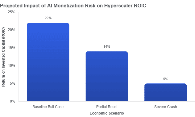
- Stranded Capital: The specialized power, liquid cooling systems, and electrical equipment tailored for dense AI clusters cannot easily be repurposed for traditional cloud workloads without lowering returns on invested capital (ROIC).
| Financial Metric | Baseline Forecast (Bull Case) | Partial Monetization Reset | Severe Crash / Structural Downside |
|---|---|---|---|
| Cloud Revenue Growth | Accelerated (driven by AI APIs & enterprise seats) | Flattens out as enterprise customers consolidate suppliers | Decelerates sharply; circular cloud revenue loops collapse |
| CapEx Infrastructure | Full execution of Dell’Oro’s ~200 GW build out by 2030 | 20–30% of capacity commitments deferred or resized | Mass cancellations of orders; multi-year build freezes |
| Operating Margins | Expands as inference costs decline relative to software prices | Compresses due to underutilized GPU clusters and high DCPI fixed costs | Severe contraction; massive asset write-downs and depreciation drag |
| ROIC | Historic highs driven by high-density compute demand | Diluted; longer payback periods for specialized data centers | Tanks; billions in stranded physical capital and obsolete hardware |
References:
https://www.nytimes.com/2026/08/10/business/ai-nvidia-lenders-500-billion.html
https://www.wheresyoured.at/dont-look-up/
Curmudgeon: Caveat Emptor: Huge Debt and Circular Financing Deals Dominate AI Build-Outs (07/23/26)
Merry-go-round of dog chasing its tail: Relationship between U.S. hyperscalers and private Gen AI companies
AI infrastructure spending boom: a path towards AGI or speculative bubble?
Expose: AI is more than a bubble; it’s a data center debt bomb
Will Google Cloud’s AI and data analytics revenue +TPU IP licensing income offset huge AI CAPEX to produce a decent ROI?
Amazon’s Jeff Bezos at Italian Tech Week: “AI is a kind of industrial bubble”
Big Tech AI spending binge results in massive job cuts!
AI spending boom accelerates: Big tech to invest an aggregate of $400 billion in 2025; much more in 2026!
FT: Scale of AI private company valuations dwarfs dot-com boom
Big tech spending on AI data centers and infrastructure vs the fiber optic buildout during the dot-com boom (& bust)
AI Data Center Boom Carries Huge Default and Demand Risks
Can the debt fueling the new wave of AI infrastructure buildouts ever be repaid?
Gartner: AI spending >$2 trillion in 2026 driven by hyperscalers data center investments
Will billions of dollars big tech is spending on Gen AI data centers produce a decent ROI?
Ericsson leads SK Telecom AI RAN vs. NVIDIA’s GPU centric AI RAN Alliance
Executive Summary:
Ericsson says it has been selected as the sole global technology partner in SK Telecom’s consortium for Korea’s Hyper-AI Network Infrastructure Demonstration Project, a South Korea government-backed initiative led by the Ministry of Science and ICT and the National Information Society Agency. The program is intended to validate AI-RAN pilot networks as a cornerstone of Korea’s national “AI Highway” strategy and its longer-term 6G roadmap.
Ericsson’s contribution [1.] to this project centers on the RAN and the automation layer that surrounds it. According to Ericsson, its role in the project includes 5G Standalone expertise, AI-in-RAN capabilities, and intelligent network automation through the Ericsson Intelligent Automation Platform (EIAP) and AI-powered rApps, enabling autonomous control, resource orchestration, and real-time optimization for physical AI services. Ericsson is not being positioned as a general AI infrastructure provider, but as the core network technology partner bringing telco-grade RAN, automation, and orchestration into a live industrial validation environment. Ericsson will contribute what it calls an “end-to-end network foundation” to the project that is intended to connect and continuously optimize intelligent machines and autonomous industrial operations. In the second phase of the project, Ericsson’s AI-RAN pilot network is expected to be applied to a real-world logistics environment at KG Mobility’s Pyeongtaek plant.
Note 1. It’s interesting to note that Ericsson is a founding member of the Nvidia GPU centric AI-RAN Alliance, contributing the operator-centric “AI-for-RAN” perspective by embedding telco-grade AI into basebands and radios to improve network performance, automation, and energy efficiency. The company’s delegates hold leadership roles in the alliance’s working groups and technical committees.
For telecom operators, the significance is not just radio performance but the shift toward a network architecture that can support physical AI use cases with tighter latency, stronger uplink capacity, and higher service assurance. SK Telecom plans to demonstrate AI-RAN pilots through 2027 across scenarios such as autonomous transport, industrial safety monitoring, and humanoid robotics, with a second-phase deployment targeted for KG Mobility’s Pyeongtaek plant.
Sibel Tombaz, Head of Customer Unit Korea, Ericsson, says: “Being selected as a key global technology partner in this government-backed Hyper-AI Network consortium is a significant recognition of Ericsson’s technology leadership and our long-term partnership with SK Telecom. Korea is moving with clear ambition to shape the future of AI-native networks and 6G, and Ericsson is proud to contribute our global expertise in 5G, AI-RAN, orchestration, and intelligent network automation to this important national initiative. We look forward to working closely with SK Telecom and the consortium partners to help turn Korea’s 6G vision into real industrial value.”
Takki Yu, VP and Head of Network R&D at SK Telecom, says: “As a key national project supporting Korea’s Hyper-AI Network strategy, SK Telecom is pleased to collaborate with Ericsson as a key technology partner to advance AI-RAN technology through global cooperation. Together, we aim to build a strategic win-win partnership, demonstrate real industrial value, and help strengthen Korea’s AI-RAN technology capabilities and ecosystem for the future.”
Comparison with NVIDIA GPU centric AI-RAN Alliance:
The SK Telecom–Ericsson initiative and the NVIDIA-led AI-RAN ecosystem share a common thesis: the RAN is evolving into a distributed compute platform that can host or coordinate AI workloads closer to where data is generated. But they emphasize different layers of the stack. SK Telecom’s Ericsson-led project is centered on operator-grade RAN validation, network autonomy, and physical AI service delivery in industrial settings, while NVIDIA’s effort is broader and more compute-centric, tied to AI factories, GPU infrastructure, and open 6G ecosystem development.
- NVIDIA is a founding member of the AI-RAN Alliance and acts as one of its most visible technical drivers, contributing reference architectures and accelerated-computing platforms for AI-RAN.
- Ericsson is the operator-focused RAN technology partner proving AI-RAN in live telco and industrial network deployments.
The practical takeaway is that Ericsson’s role is more narrowly telecom-native, while NVIDIA’s consortium is more infrastructure- and compute-oriented. For 6G, the two approaches are complementary rather than contradictory: one is proving how the network behaves as a deterministic industrial platform, the other is building the compute substrate that can feed AI-native services into that platform.ericsson+2
Why it matters:
SKT announced the Hyper-AI Network Infrastructure Development project last month, and at the time Ericsson, Nokia, Samsung and private mobile networking specialist HFR were named as those providing the kit and related network and software solutions.
South Korea has become one of the most advanced and competitive mobile markets, and this makes it a useful proving ground for AI-RAN. If the SK Telecom pilot succeeds, it could strengthen the case that future mobile networks must support not only connectivity, but distributed inference, orchestration, and machine control for robots, vehicles, and industrial systems.
From a standards and market perspective, the more interesting question is how these pilots influence the eventual division of labor between RAN, edge compute, and centralized AI infrastructure in 6G-era networks. That is where the SK Telecom–Ericsson model, with its operator-led network validation, may prove especially influential.
…………………………………………………………………………………………………………………………………………………………………………………………………
References:
https://www.ericsson.com/en/press-releases/2026/8/skt-hyper-ai-consortium
https://www.telecoms.com/ai/ericsson-named-sole-global-vendor-for-sk-telecom-s-hyper-ai-consortium
Ericsson goes with custom silicon (rather than Nvidia GPUs) for AI RAN
Dell’Oro: AI RAN revenue forecast: $35B from 2026-to-2030; 3 types of AI RAN explained
Dell’Oro: RAN Market Stabilized in 2025 with 1% CAG forecast over next 5 years; Opinion on AI RAN, 5G Advanced, 6G RAN/Core risks
Dell’Oro: Analysis of the Nokia-NVIDIA-partnership on AI RAN
RAN silicon rethink – from purpose built products & ASICs to general purpose processors or GPUs for vRAN & AI RAN
Dell’Oro: AI RAN to account for 1/3 of RAN market by 2029; AI RAN Alliance membership increases but few telcos have joined
Dell’Oro: RAN revenue growth in 1Q2025; AI RAN is a conundrum
Analysis: Nokia’s new AI-RAN platform and Standalone AI-RAN node with Nvidia GPUs
Nokia today announced what it describes as the first commercial AI-RAN platform, signaling a potentially significant inflection point in radio access network architecture. As AI workloads increasingly influence network design and operations, service providers are under pressure to deliver higher capacity, improved cost efficiency, and faster service innovation without depending on traditional hardware refresh cycles. Nokia’s AI-RAN platform is positioned to address these requirements by extracting greater uplink and downlink performance from existing spectrum and radio assets, while enabling a transition toward AI-native network architectures through software-centric evolution. Key take-aways:
- Nokia launches the industry’s first commercial AI-RAN platform, turning AI-RAN from vision into reality and providing a practical path to AI-native networks.
- Built on Nokia’s AI-native anyRAN software and NVIDIA’s Aerial AI-RAN platform, it will deliver more than 100% spectral efficiency gains by 2028, doubling the capacity of existing spectrum assets.
- Nokia’s anyRAN software will support three new accelerated computing baseband platforms. In addition, its existing portfolio will be fully ORAN compliant so operators can modernize at their own pace.
“AI-RAN is the biggest innovation in radio in decades. AI-RAN makes the network intelligent, extends AI into the physical world, and allows telcos to get more from their existing infrastructure, including a software upgrade path to 6G. Nokia’s anyRAN software, powered by NVIDIA’s Aerial AI-RAN platform, unlocks greater performance from the spectrum operators already have and can be deployed with existing Nokia or ORAN-compliant radio units. For operators, that means more performance, better returns and faster delivery of new services,” said Justin Hotard, President and Chief Executive Officer at Nokia.
The platform is built on Nokia’s AI-native network architecture and leverages NVIDIA’s accelerated computing stack to enable AI-driven radio optimization. Initial results indicate spectral efficiency gains exceeding 20% through AI-enhanced radio resource management and signal processing techniques. Nokia’s roadmap targets up to 50% gains by 2027 and greater than 100% by 2028, with the objective of increasing capacity in dense deployments while reducing cost per bit and improving user experience.
“Telecommunications is entering the AI era — the radio access network is the next AI infrastructure,” said Jensen Huang, CEO and founder of NVIDIA. “Together with Nokia, we are bringing NVIDIA CUDA and AI into the baseband, transforming RAN into a planet-scale AI computer. This is a generational shift for operators — unlocking more capacity and efficiency from today’s spectrum while creating the foundation for new AI services and the 6G era.”
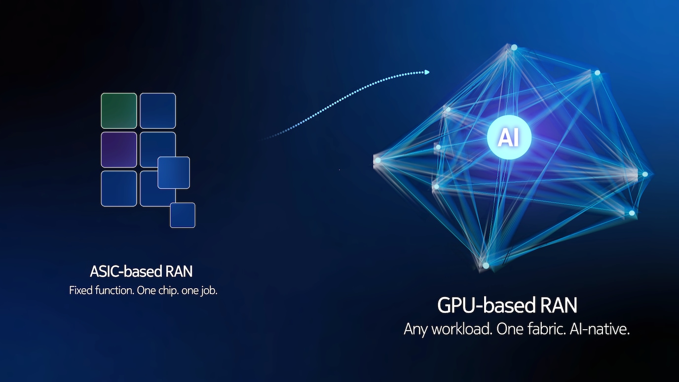
Image credit: Nokia
A key element of the offering is a software subscription model that enables operators to access ongoing AI-driven enhancements, feature updates, and performance improvements independent of hardware upgrade cycles. Nokia expects pilot deployments to begin by the end of the year, with broader commercial availability targeted for 2027. The roadmap incorporates NVIDIA’s programmable merchant silicon to support continued performance scaling and feature evolution.
“Nokia’s AI-RAN launch represents an important step in bringing AI-RAN from industry vision to commercial reality. The addition of the new AI-RAN node alongside the AirScale capacity plug-in unit and cloud-native deployment options gives operators practical choices for adopting AI-native networks based on their existing infrastructure and transformation goals. By combining AI-accelerated computing with a software-defined architecture and a clear product roadmap, Nokia is helping operators unlock greater capacity, improve network economics and accelerate the transition toward AI-native RAN,” commented Rémy Pascal, Practice Leader, Mobile Infrastructure at Omdia.
Light Reading’s Iain Morris wrote:
Nokia’s vision, outlined during an exclusive interview with Light Reading, is that the Nvidia-based hardware products announced today and available from next year will potentially last customers deep into the 6G era. That cannot be said of the latest Nokia hardware in commercial use, based on custom silicon provided by Marvell Technology, according to Atkinson. The same would be true of the latest hardware from rival Ericsson, he believes: “It will get them into 6G, but it won’t see them long into 6G.”
The Nokia pivot to GPUs sets up a riveting clash between the two Nordic companies. Ericsson remains firmly attached to its own custom silicon, and its top executives think writing code for CUDA, Nvidia’s software platform, could make Nokia a victim of “vendor lock-in,” imprisoned by a single vendor’s hardware.
For telcos interested in general-purpose processors and the greater freedom they promise, Ericsson instead offers a set of “virtual” RAN products. While based today on Intel’s central processing units (CPUs), the same software can run on CPUs from other chipmakers after minimal tweaks, according to Ericsson. Only a small amount of code remains hardware-dependent, it says.
,,,,,,,,,,,,,,,,,,,,,,,,,,,,,,,,,,,,,,,,,,,,,,,,,,,,,,,,,,,,,,,,,,,,,,,,,,,,,,,,,,,,,,,,,,,,,,,,,,,,,,,,,,,,,,,,,,,,,,,,,,,,,,,,,,,,,,,,,,,,,,,,,,,,,,,,,,,,,,,,,,,,,,,,,,,,
Nokia’s AI-RAN platform is based on a common, software-defined architecture integrating its anyRAN software with NVIDIA’s accelerated computing. The platform supports 4G, 5G, and forward evolution toward 6G, while maintaining compliance with Open RAN specifications to enable multi-vendor interoperability. Operators can select from multiple deployment options aligned with their installed base and transformation strategy, while leveraging a unified software roadmap.
For network operators with existing Nokia AirScale deployments, the introduction of a GPU-accelerated capacity plug-in unit provides a relatively low-friction upgrade path. This approach integrates accelerated computing into the current RAN footprint, enabling step-function capacity improvements while preserving prior infrastructure investments. Nokia also highlights support for AI-optimized merchant silicon, including contributions from partners such as Marvell, reflecting a broader ecosystem strategy for AI-RAN evolution.
Nokia is also introducing a GPU-based standalone AI-RAN node designed for flexible deployment across diverse network environments. The platform supports 4G, 5G, and future 6G workloads and can be deployed as a discrete node, in clustered configurations, or integrated with existing AirScale systems as a logical baseband. This enables scalable deployment of AI-native capacity while maintaining architectural flexibility.
For network operators pursuing cloud-native RAN strategies, Nokia’s AI-RAN capabilities extend to GPU-enabled COTS server platforms delivered through ecosystem partners. This approach supports deployment on standardized, accelerated infrastructure while aligning with open and secure supply chain principles. It combines cloud-native operational models with the performance requirements of AI-intensive RAN workloads.
Nokia’s AI-RAN introduces a shift from hardware-centric lifecycle management to a software-driven innovation model. Through its subscription-based framework, operators gain continuous access to evolving AI algorithms, spectral efficiency enhancements, and network optimization capabilities. This model enables ongoing improvements in performance, efficiency, security, and resilience without requiring discrete hardware upgrades, thereby improving total cost of ownership and extending asset lifecycles.
By combining AI-accelerated computing, software-defined RAN architecture, and an open ecosystem approach, Nokia’s AI-RAN platform is intended to provide operators with a scalable pathway to increased capacity, improved economic performance, and continuous innovation as networks evolve toward the 6G era.
References:
https://www.nokia.com/radio-access/ai-ran/
https://www.lightreading.com/6g/nokia-says-long-term-6g-is-not-doable-without-nvidia
Analysis: Nvidia’s rumored new 6G AI-RAN – likely features/functions and industry impact
Executive Summary:
According to Light Reading, Nvidia is working on a GPU combo chip that would sit directly in the 6G radio unit [1.], extending its AI-RAN push from baseband/server into the radio itself. It’s reported to be a more hardware-integrated, sub-100W embedded design rather than just GPU acceleration in centralized RAN compute.
Note 1. 6G/IMT 2030 Radio Interface Technologies (RITs) have yet to be defined, let alone specified by 3GPP or ITU-R WP5D. They won’t be solidified until the end of 2030 so any specific silicon design won’t be completed until then or 2031!
……………………………………………………………………………………………………………………………………………………….
Light Reading’s headline frames it as a “radical new AI-RAN plan and they wrote that “the move was confirmed by knowledgeable sources, with Nvidia saying GPUs in more advanced radios will become “essential” in future. It marks a dramatic new development in the GPU giant’s “AI-RAN” strategy.”
If accurate, this would be a notable shift for Nvidia, because it would let them influence the whole RAN stack, not just centralized compute. That could matter for performance, power efficiency, and AI-native functions such as sensing, spectrum optimization, and real-time signal processing. Nvidia’s broader 6G messaging already emphasizes AI-native wireless, integrated sensing and communications, and spectrum agility as core themes.
The unconfirmed report fits Nvidia’s existing telecom roadmap rather than appearing out of nowhere. Nvidia has already announced an AI-native wireless stack for 6G with partners including Cisco, MITRE, Booz Allen, ODC, and T-Mobile, and it has promoted AI-RAN as a way to combine connectivity, computing, and sensing on one platform. It also aligns with the company’s recent partnership with Nokia, where Nvidia introduced the ARC-Pro 6G-ready accelerated computing platform and described it as a software-upgradable path from 5G-Advanced to 6G. That makes the rumored radio-chip move look like a vertical extension of the same strategy.
For wireless network operators, a radio-unit chip from Nvidia would be significant only if it improves cost, power, or flexibility versus incumbent RU silicon. The practical test will be whether it can deliver enough RF, baseband, and AI function integration to justify another architecture layer at the edge. It would also intensify competition in the radio-access supply chain and reinforce the trend toward AI-native, software-defined RANs. It also suggests Nvidia wants to shape not only the compute layer but the physical radio layer of 6G networks.
Possible AI Silicon Features and Functions:
Nvidia would most likely add AI-for-RAN features into radio silicon first, because those map directly to signal processing and link adaptation rather than to generic “AI at the edge.” Nvidia’s own AI-RAN materials emphasize embedding AI/ML into the radio signal-processing layer to improve spectral efficiency, coverage, capacity, and performance. Here are a few likely AI features/functions for the rumored 6G AI Nvidia super chip:
-
Neural channel estimation and equalization, to infer cleaner channel state from noisy RF observations and improve link reliability. Nvidia’s open-source Aerial release specifically calls out advanced neural models for channel estimation.
-
Real-time beam management, including beam selection, beam tracking, and beam refinement for massive MIMO and mmWave/upper-midband deployments. These are natural AI-RAN use cases because they depend on fast adaptation to changing propagation conditions.
-
Spectrum agility and interference mitigation, such as identifying jammed or congested resource blocks and dynamically avoiding them. NVIDIA and partners have already described spectrum agility applications that freeze only affected frequencies while keeping the rest of the system online.
-
Dynamic resource scheduling, using learned traffic and channel patterns to allocate PRBs, power, and compute more efficiently in real time. Nvidia describes AI-RAN as improving spectral efficiency and dynamic traffic handling through AI.
-
Integrated sensing and communications support, where the radio helps detect objects, motion, or environmental context in parallel with communication. Nvidia has already highlighted ISAC-style applications with camera/RF fusion and object tracking.
-
Edge inference hooks, letting the RU expose real-time PHY data to AI applications or a dApp-style framework. Nvidia’s open-source Aerial stack says third-party apps can access physical-layer data through secure APIs and modify RAN behavior in real time.
-
Self-optimization and closed-loop control, where the radio silicon learns local conditions and continuously retunes thresholds, coding, MCS selection, and precoding policies. That fits Nvidia’s broader framing of AI-native networks as software-defined and continuously adaptable.
The most plausible first wave is not a fully autonomous “AI radio,” but a hybrid RU chip that accelerates selected PHY functions and exposes telemetry/data paths to the rest of the AI-RAN stack. Nvidia’s current messaging emphasizes software-defined infrastructure, deterministic performance, and layered AI-RAN capabilities rather than replacing the entire RAN with a black-box model.
The real differentiator would be whether Nvidia can combine RF signal processing with its GPU/CUDA ecosystem, so the same platform handles channel learning, inference, and orchestration across RU/DU/CU tiers. That would let operators optimize for spectral efficiency and OPEX while still keeping a software-upgrade path to 6G. Radio electronics is constrained by power, latency, determinism, and certification, so Nvidia would need to prove these AI features help without destabilizing PHY timing. That is why the likely starting point is assistive AI inside the signal chain, not a fully learned end-to-end radio.
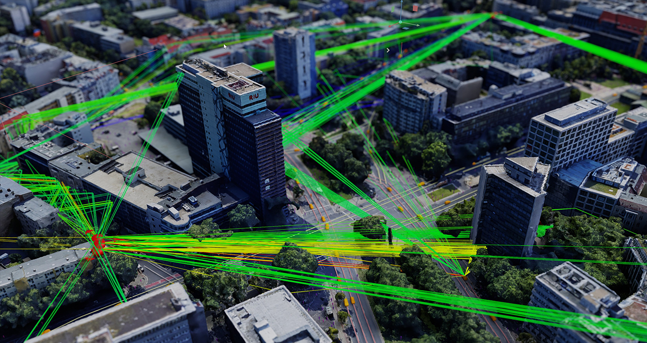
Image Credit: Nvidia
…………………………………………………………………………………………………………………………………………………………………………………………………………..
Competitive Analysis:
Nvidia’s reported move into a 6G radio-unit chip is most threatening to Marvell and Qualcomm at the silicon layer, while it is more of a strategic architecture challenge to Nokia and Ericsson at the system level. The immediate effect is less about a single chip and more about Nvidia trying to pull compute, connectivity, and AI deeper into the RAN value chain
Qualcomm is the closest direct competitor if Nvidia is trying to put silicon into the radio or near-radio layer. Qualcomm already has a Layer 1 strategy that combines silicon and software in SmartNIC/server-adjacent form factors, so Nvidia would be moving into a space where Qualcomm has both telecom credibility and established IP.
The risk for Qualcomm is that Nvidia can use its AI brand, CUDA ecosystem, and hyperscale relationships to redefine what “performance” means in RAN silicon, especially if AI-native functions become a buying criterion. The counterpoint is that Qualcomm still has a strong edge in wireless-specific silicon integration and standards heritage, which matters if the 6G radio path remains RF- and modem-centric.
Nokia looks less exposed in the short term because it is already partnering with Nvidia rather than treating it as a pure adversary. Nvidia and Nokia have publicly framed their relationship as an AI-native 5G-Advanced/6G platform effort, and Nokia says it will add NVIDIA-powered commercial AI-RAN products to its RAN portfolio.
Nonetheless, a Nvidia radio-chip push could still compress Nokia’s differentiation over time if more of the RAN stack becomes software-defined and GPU-centric. The strategic question is whether Nokia remains the integrator and operator-facing systems vendor, or whether Nvidia gradually becomes the architectural center of gravity.
Ericsson is the most structurally interesting case because it sits at the high end of global RAN share and has been more cautious about Nvidia as a Layer 1 option. Light Reading notes Ericsson is currently dismissive of Nvidia as a Layer 1 choice, even while the broader ecosystem explores AI-RAN collaboration.
For Ericsson, the threat is not immediate revenue loss from a single chip; it is erosion of the traditional assumption that RAN leadership comes from proprietary radio and baseband stacks. If Nvidia can make AI-native RAN a default design paradigm, Ericsson may be forced to defend its software and systems value rather than simply its box-selling model.
Samsung Electronics contacted Light Reading after their story was published to point out that it also works with AMD as a chip partner. “Samsung supports full Layer 1 (L1) processing using Intel’s telco CPUs (e.g., Xeon 6 Granite Rapids) and lookaside accelerator approach and in addition has successfully demonstrated full L1 processing on AMD’s CPUs without relying on dedicated L1 accelerators,” a Samsung spokesperson said via email.
Marvell is the most exposed chip supplier in this story because its telecom position is more concentrated in custom Layer 1 silicon. Light Reading specifically points out that Marvell is a critical supplier to Nokia in Layer 1, which makes a Nvidia radio-chip effort a direct substitution threat in portions of the stack.
If Nvidia succeeds, Marvell faces a two-sided squeeze: loss of design wins in telecom silicon and a narrative shift toward AI-native programmable platforms that favor Nvidia’s broader ecosystem. Marvell’s defense is that telecom operators still care about power, latency, and deterministic functionality, areas where custom silicon can remain more efficient than a generalized AI-compute approach.
…………………………………………………………………………………………………………………………………………………………………………
Summary Table:
| Company | Impact level | Why |
|---|---|---|
| Qualcomm | High | Direct silicon adjacency and overlapping Layer 1 ambitions. |
| Marvell | High | Telecom custom-silicon exposure, especially Layer 1. |
| Ericsson | Medium | Strategic and architectural threat more than immediate chip displacement. |
| Nokia | Medium to low near term | Partnered with Nvidia, so risk is more about future dependence and stack control. |
Source: Perplexity.ai
…………………………………………………………………………………………………………………………………………………………………………
Conclusions:
It’s unknown whether Nvidia’s rumored radio chip becomes a product, a reference design, or just an extension of its AI-RAN platform. If it ships, watch for operator trials, power-envelope disclosures, and whether it targets RU integration, DU acceleration, or a hybrid AI-RAN endpoint. If it stays at the partnership/reference-design level, the market impact will be more narrative than revenue-relevant.
Another unanswered question is whether Nokia and Ericsson keep treating Nvidia as a collaborator while preserving their own Physical layer control, or whether they start to see Nvidia as a platform owner in the making. That boundary will determine whether this is a tactical ecosystem play or the beginning of a deeper industry reset.
…………………………………………………………………………………………………………………………………………………………………………
References:
https://www.lightreading.com/6g/nvidia-has-a-radical-new-ai-ran-plan-a-6g-radio-unit-chip
https://www.lightreading.com/6g/analyst-insight-6g-coming-into-focus
https://www.nvidia.com/en-us/industries/telecommunications/ai-ran/
RAN Silicon Rethink- Part II; vRAN and General-Purpose Compute
Orange, Nokia, Nvidia, and Intel debate: ASICs vs. GPUs vs. General-Purpose CPUs for RAN Baseband Processing
RAN silicon rethink – from purpose built products & ASICs to general purpose processors or GPUs for vRAN & AI RAN
Dell’Oro: Analysis of the Nokia-NVIDIA-partnership on AI RAN
Nvidia pays $1 billion for a stake in Nokia to collaborate on AI networking solutions
Inside Nokia’s new AI Networking Innovation Lab
Analysis: Nvidia’s $2 billion investment in Marvell; NVLink Fusion ecosystem & RAN vendor silicon strategy
Marvell shrinking share of the RAN custom silicon market & acquisition of XConn Technologies for AI data center connectivity
Nvidia strategic partnership with IREN targets 5G Watts AI infrastructure buildout + $2.1B investment option
Nvidia has announced a strategic partnership with cloud AI data center operator IREN [1.] to deploy up to 5G Watts (5GW) of AI infrastructure, driven by a $3.4 billion services contract and a $2.1 billion investment option for Nvidia. This collaboration aims to secure critical, high-density data center capacity for AI workloads while accelerating IREN’s transition into a major AI infrastructure provider. This strategic expansion targets up to 5GW of NVIDIA DSX-aligned AI infrastructure across IREN’s global pipeline. The roadmap centers on the 2GW Sweetwater campus in Texas, positioned to be the flagship deployment of NVIDIA’s DSX factory architecture. This integrated model synergizes NVIDIA’s reference designs with IREN’s core competencies in utility-scale power procurement, site development, and full-stack GPU cloud operations.
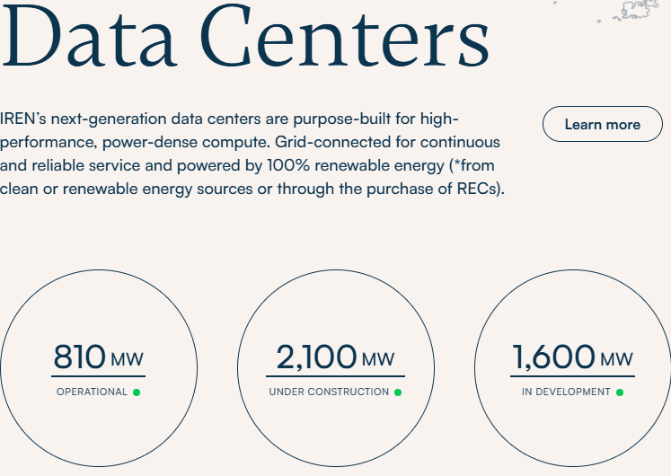
“AI factories are becoming foundational infrastructure for the global economy,” said Jensen Huang, founder and CEO of Nvidia. “Deploying these systems at scale requires deep integration across the full stack — compute, networking, software, power and operations. IREN brings the scale and infrastructure expertise to help accelerate the buildout of next-generation AI infrastructure globally. Together, we are building for the age of AI,” he added. Future deployments are expected to focus on IREN’s 2-gigawatt Sweetwater campus in Texas, which the companies expect to serve as a flagship deployment for Nvidia’s DSX architecture.
“This partnership combines NVIDIA’s AI systems and architecture leadership with IREN’s expertise across power, land, data centers, GPU deployment and infrastructure operations,” said Daniel Roberts, cofounder and co-CEO of IREN. “Together, we believe we can accelerate deployment of AI infrastructure and expand access to compute for AI-native and enterprise customers globally.”
References:
China vs U.S.: Race to Generate Power for AI Data Centers as Electricity Demand Soars
Fiber Optic Boost: Corning and Meta in multiyear $6 billion deal to accelerate U.S data center buildout
How will fiber and equipment vendors meet the increased demand for fiber optics in 2026 due to AI data center buildouts?
Big tech spending on AI data centers and infrastructure vs the fiber optic buildout during the dot-com boom (& bust)
Analysis: Cisco, HPE/Juniper, and Nvidia network equipment for AI data centers
Expose: AI is more than a bubble; it’s a data center debt bomb
Can the debt fueling the new wave of AI infrastructure buildouts ever be repaid?
Orange, Nokia, Nvidia, and Intel debate: ASICs vs. GPUs vs. General-Purpose CPUs for RAN Baseband Processing
For Orange CTO Laurent Leboucher, the main attraction of AI today lies in its potential to improve the efficiency of 5G radio access networks (RANs). That helps explain Orange’s recent collaboration with Nokia and Nvidia. Orange already deploys Nokia’s purpose-built 5G network equipment and software at mobile sites in France and other markets. Until recently, it had little obvious need for Nvidia, the U.S. chip making king best known for the graphics processing units (GPUs) used to train large language models. But Nokia and Nvidia became closely aligned last October, when Nvidia took a 3% stake in Nokia as part of a $1 billion investment. Nokia is now developing AI RAN software designed to run on GPUs.
Leboucher’s interest is driven in part by concerns over the cost of custom silicon — the application-specific integrated circuits (ASICs) used in purpose-built 5G networks. “It creates an opportunity to bring a general-purpose chipset instead of an ASIC implementation,” he told Light Reading at last week’s FutureNet World event in London. “I think we could, at some point, benefit from the economies of scale of new chipsets. That could be Nvidia.”
The rationale is much easier to understand than arguments about 5G for autonomous vehicles. Chip manufacturing is already expensive, and both Nokia and Ericsson expect component costs to rise further this year amid relentless AI demand. At the same time, the RAN market remains relatively small and has contracted. According to market research firm Omdia, telco spending fell from $45 billion in 2022 to $35 billion last year and is expected to stay at that level. In that context, it is increasingly difficult to justify designing high-cost chips with limited reuse outside telecom.

Image Credit: Orange
Last year, Nvidia spent about $18.5 billion on research and development, generated nearly $216 billion in revenue, and reported a gross margin of more than 70%. Its financial strength is not in question. If telecom operators can use its GPUs for RAN software, they may face less pressure to secure the long-term economics of 5G and 6G development. That alone could be enough to support the case for Nvidia. The counterarguments are cost and power consumption. By design, custom silicon is optimized for a specific workload and will always outperform a more general-purpose processor at that task. An Nvidia GPU in the RAN could therefore be seen as excessive — like using a crop duster to water a hanging basket.
Leboucher, believes that Nokia and Nvidia are developing something far more compact than a typical data-center deployment. “It is not a Blackwell GPU,” he said, referring to Nvidia’s current hyperscaler-class product line. “I have an understanding it’s something which is a little bit smaller.” One of the first GPU-based products is expected to come on a card that Orange can insert into an existing Nokia AirScale chassis.
He is also interested in replacing traditional RAN algorithms with AI to improve spectral efficiency and overall performance. Through trials with Nokia and Nvidia, Orange wants to determine whether a GPU is actually required to capture the full benefit. “We can completely rethink the way we are doing algorithms today, using AI for the radio Layer 1,” he said, referring to the most compute-intensive part of the RAN software stack. Some of the “AI-RAN” narrative still sounds “a little bit like science fiction,” Leboucher admitted. “But I think there are some very interesting ideas behind that. We want to understand where we are.”
This is not the first time the industry has debated a shift from ASICs to general-purpose processors for RAN equipment. Alongside its purpose-built 5G portfolio, Ericsson already offers cloud RAN products based on Intel CPUs. Samsung is now focused on Intel-based virtual RAN and has recently predicted the end of purpose-built 5G. Even so, cloud and virtual RAN still account for only a small share of live 5G deployments. Huawei and Ericsson, the two largest RAN vendors, remain committed to custom silicon development.
Nvidia’s entry into the market has clearly given Leboucher and his team more to evaluate as RAN technology becomes more sophisticated. “We are introducing new requirements for radio networks, typically for beamforming, and we have to consider the need for quite powerful chipsets,” he said. “Whether the best way to keep going is using ASICs or a general-purpose architecture – I think this is a good time to ask the question. Before, it was too early.”
The answer could shape Orange’s next major RAN decisions. The operator is preparing for what Leboucher describes as a “refresh” of RAN equipment across several countries ahead of the expected 6G launch in 2030. For the first time, he said, Orange will include cloud RAN as a “major option” in its request for proposal.
The concern around Intel as an alternative to Nvidia is its still-fragile financial position. Before December, Intel had been trying to spin off its network and edge group (NEX), which develops RAN chips. Those plans were later shelved, but the company’s net loss widened to about $4.3 billion in the most recent first quarter, from $887 million a year earlier, while revenue rose only 7% year over year to $13.6 billion. Cristina Rodriguez, who had led NEX, left this month to join Coherent, and Intel has not yet named a successor. “The shares jumped 28% in after-hours trading, taking Intel firmly into meme-stock territory,” said Radio Free Mobile analyst Richard Windsor in a blog published after results came out on April 23. “I say meme-stock because there is no other way to describe it when the shares are on a 2026 PER [price-to-earnings ratio] of 137x, and its technology looks obsolete.”
Orange places significant value on separating hardware from software, allowing the same RAN software to run across multiple hardware platforms. Ericsson and Samsung both say the virtual RAN software they have built for Intel CPUs could, with relatively modest changes, be ported to AMD silicon using the same x86 architecture or to Arm-based CPUs.
By contrast, Layer 1 code written for Nvidia GPUs and the CUDA software stack would not be portable to other platforms, according to Ericsson. “I think the main challenge we see with that is we are trying very hard to keep our stack portable, to give hardware options,” Michael Begley, Ericsson’s head of RAN compute, told Light Reading at MWC Barcelona this year. “If you go all in on one, it’s great, but you’re all in on one, and you can’t offer those other options to the operators or the ecosystem.”
Leboucher acknowledges that risk. “The risk of lock-in exists, definitely,” he said. “We really want to stay open. At the same time, we know that benefiting from a very, very large-scale general-purpose architecture should improve the TCO [total cost of ownership]. At the end of the day, it will be a trade-off. But we would welcome an architecture where we have the capacity at some point to decide to swap if we need to swap.”
Nokia’s hope is that much of the Layer 1 software written for Nvidia GPUs will eventually be deployable on other GPU platforms. But Nvidia’s near-monopoly in that segment leaves the industry with few alternatives for now. There is also optimism inside Nokia that GPU-based code could later be adapted for capable CPUs, although Ericsson’s comments suggest that would be much harder. For telecom executives, the choices made over the next couple of years may be pivotal as 6G approaches.
………………………………………………………………………………………………………………………………………………………
References:
https://www.lightreading.com/5g/orange-weighs-nvidia-against-intel-for-5g-chips-ahead-of-new-rfp
RAN Silicon Rethink- Part II; vRAN and General-Purpose Compute
RAN silicon rethink – from purpose built products & ASICs to general purpose processors or GPUs for vRAN & AI RAN
Analysis: Nokia and Marvell partnership to develop 5G RAN silicon technology + other Nokia moves
Analysis: Nvidia’s $2 billion investment in Marvell; NVLink Fusion ecosystem & RAN vendor silicon strategy
Ericsson goes with custom silicon (rather than Nvidia GPUs) for AI RAN
Marvell shrinking share of the RAN custom silicon market & acquisition of XConn Technologies for AI data center connectivity
Custom AI Chips: Powering the next wave of Intelligent Computing
OpenAI and Broadcom in $10B deal to make custom AI chips
Will Google Cloud’s AI and data analytics revenue +TPU IP licensing income offset huge AI CAPEX to produce a decent ROI?
Big Tech AI spending binge results in massive job cuts!
Analysis: Nvidia’s $2 billion investment in Marvell; NVLink Fusion ecosystem & RAN vendor silicon strategy
NVIDIA just announced a $2 billion investment in custom silicon developer Marvell Technology (NASDAQ:MRVL). This comes right on the heels of its $2 billion investments in Lumentum, Coherent, and $1 billion in Nokia.
- NVIDIA is also deepening its relationship with Marvell within its NVLink Fusion ecosystem. NVLink is NVIDIA’s proprietary scale-up networking system. Scale-up refers to connecting computing components within a rack rather than between racks.
- NVLink Fusion essentially allows customers to connect non-NVIDIA components to NVIDIA components within the same rack. Thus, customers can mix and match technologies from different vendors when they make a purchase. However, each platform does need to have at least one NVIDIA component.
- NVLink Fusion is in opposition to the UALink consortium, of which NVIDIA is not a member. Key NVIDIA competitors like Broadcom (NASDAQ:AVGO) and Advanced Micro Devices (NASDAQ:AMD) back UALink. Companies in this group have the same goal as NVIDIA does for NVLink Fusion: to allow customers to easily connect their devices together within racks.
- UALink’s goal is to reduce NVIDIA’s power by providing an alternative to NVLink Fusion. One of the key benefits to data center operators, which buy AI chips, is avoiding vendor lock-in. By being able to source components from a wide range of companies, there is greater competitive pressure, and thus more room to negotiate. Building AI infrastructure solely on NVLink grants NVIDIA massive bargaining power.
Photo Credit: Marvell Technology
Marvell has been a member of both NVLink and UALink, one of the few major chip companies that can make this claim. Now, NVIDIA is more formally recognizing Marvell’s place within NVLink, potentially expanding its ability to win customers. Meanwhile, Marvell strengthens its standing in the AI market. From Marvell’s perspective, the deal has significant benefits. Even though Marvell was already a part of NVLink Fusion, the company’s place within this ecosystem is now elevated. Not all companies in NVLink Fusion have received a multi-billion-dollar investment from NVIDIA or their own dedicated announcement.
These factors suggest that NVIDIA is particularly confident in Marvell’s solutions and that it will put in more effort to sell them to customers. NVIDIA now has 2 billion more reasons to do just that. This is particularly noteworthy, as MediaTek and Alchip Technologies are also in NVLink Fusion, and compete with Marvell in custom silicon.
In fact, Alchip has been the source of considerable volatility in Marvell shares over the recent past. This comes as some investors believed that the firm would siphon off much of the custom chip business that Marvell has built with Amazon. However, Marvell’s last earnings report helped to significantly quell these fears. Additionally, Marvell will add $2 billion to its balance sheet. That is very significant, as the company ended last quarter with cash and equivalents of just $2.64 billion, adding meaningful financial flexibility.
The announcement also outlines new products outside of custom silicon that NVIDIA and Marvell will collaborate on. This includes scale-up networking components, optical interconnect solutions, and silicon photonics. This comes just two months after Marvell completed its acquisition of Celestial AI, which it calls a “pioneer in optical interconnect technology for scale-up connectivity.”
Expanding the language of the partnership to include these very products suggests that NVLink Fusion could offer a significant pathway to grow this recently acquired business. Overall, between the $2 billion investment, the dedicated announcement, and the expanded partnership scope, Marvell now looks like the custom silicon provider of choice within NVLink Fusion.
NVIDIA is telling its customers that its technology and Marvell’s can integrate seamlessly. This could influence future customers who want to use both products to do so on NVLink. As a result, the firm could see revenue benefits by getting in on deals it otherwise might not have participated in. This logic extends to customers interested in Marvell’s optical interconnect and scale-up solutions.
……………………………………………………………………………………………………………………………………………………………………………………………………………………………..
RAN Silicon Strategy:
- Ericsson continues to prioritize its in-house custom ASICs, dismissing claims that the R&D required is unsustainable. Michael Begley, Ericsson’s Head of RAN Compute, noted at MWC that their 30-year legacy of iterative development creates a cost efficiency that a “blank sheet” competitor couldn’t match.. Despite this, Ericsson is diversifying through its Cloud RAN portfolio. Their vRAN software, currently optimized for Intel x86 architectures, is being architected for portability across AMD and Nvidia (Arm-based) platforms. While Ericsson frames this as addressing varied customer requirements, industry observers view it as a strategic hedge against the shifting hardware landscape.
- Conversely, Nokia is signaling a pivot away from proprietary hardware. Following a significant investment from Nvidia, Nokia’s leadership has articulated a shift toward general-purpose hardware and decoupled software models. Although Nokia remains contractually tied to Marvell for custom silicon through the mid-2030s, the potential to offload intensive Massive MIMO processing to Nvidia GPUs suggests a technical path toward phased-out reliance on traditional custom ASICs.
- Furthermore, Ericsson utilizing look-aside acceleration via custom ASICs while Nokia commits to in-line acceleration using SmartNICs for improved performance and TCO. Ericsson prioritizes in-house silicon for efficiency, whereas Nokia is shifting toward general-purpose hardware and Nvidia-backed GPU acceleration.
- Meanwhile, Samsung’s RAN silicon strategy has fundamentally inverted the traditional industry model: virtualized RAN (vRAN) is now its primary offering, with purpose-built custom silicon moved to the periphery. As of early 2026, Samsung is the global leader in vRAN deployments, surpassing 53,000 active sites. For vRAN, Samsung is aggressively diversifying its silicon partners beyond Intel to include AMD (x86) and NVIDIA (Arm-based Grace CPUs) to prevent hardware lock-in. The South Korean company is positioning its vRAN as the “AI-native” foundation for 5G-Advanced and 6G, aiming for fully autonomous “autopilot” networks by 2027 through its CognitiV NOS (Network Operations Suite).
- Samsung is leveraging its internal silicon foundry to develop 2nm Exynos chips and Silicon Photonics (“Dream Chip”), with a mass production target of 2028 to integrate optical transmission directly into AI accelerators and RAN modules. Its new Network in a Server (NIS) solution consolidates Core, vCU, vDU, and AI agents into a single 1U server, targeted at private 5G and enterprise edge use cases. While Samsung has pivoted heavily toward a vRAN-first strategy, it still maintains a portfolio of purpose-built (non-vRAN) equipment that utilizes custom ASICs. However, the role of these chips is shifting from a primary focus to a supporting role as the industry moves toward general-purpose hardware.
- Legacy and Specialized Support: Samsung continues to sell and support its traditional Baseband Units (BBUs), which are powered by proprietary silicon developed in partnership with companies like Marvell. These ASICs are still used for high-density, performance-critical deployments where standard CPUs are not yet chosen by the operator.
- Hardware Acceleration: In non-vRAN scenarios, custom ASICs handle the most computationally intensive Layer 1 (L1) tasks, such as beamforming for Massive MIMO and FEC (Forward Error Correction).
- Phased-Out Trajectory: Samsung executives have acknowledged that the era of proprietary hardware is likely nearing its end. Alok Shah, VP of Network Strategy at Samsung, has noted that while they still provide purpose-built BBUs, it is only a “matter of time” before vRAN becomes the universal standard.
……………………………………………………………………………………………………………………………………………………….
References:
https://www.lightreading.com/5g/nvidia-backed-marvell-pitches-one-chip-to-rule-the-ran
RAN Silicon Rethink- Part II; vRAN and General-Purpose Compute
RAN silicon rethink – from purpose built products & ASICs to general purpose processors or GPUs for vRAN & AI RAN
AI-RAN Reality Check: hype vs hesitation, shaky business case, no specific definition, no standards?
Ericsson goes with custom silicon (rather than Nvidia GPUs) for AI RAN
AT&T and Ericsson boost Cloud RAN performance with AI-native software running on Intel Xeon 6 SoC
Analysis: Rakuten Mobile and Intel partnership to embed AI directly into vRAN
Is the “far edge” a bridge to far to cross for AI inferencing? What about “Distributed AI Grids”?
Analysis: Edge AI and Qualcomm’s AI Program for Innovators 2026 – APAC for startups to lead in AI innovation
Will “AI at the Edge” transform telecom or be yet another telco monetization failure?