

Broadcom
Broadcom lending Anthropic up to $42 billion in yet another AI circular financing deal
Backgrounder:
According to Reuters, which obtained Anthropic’s IPO prospectus, the Big Tech giants are depicted in multiple ways in the IPO filing- as distribution partners, financial backers, computer suppliers, and competitors, all at once. They uncovered the clearest view yet of how circular the AI world really is, and how much an AI lab’s success depends on the giants it’s also competing against.
Reuters was able to calculate that Anthropic pays roughly 16% of every dollar it earns from its cloud partners (Amazon, Google, Microsoft) back to those same big tech partners. It counts the full value of contracts sold through a cloud marketplace as revenue, then treats the cloud platform’s cut of revenue as a marketing cost.
OpenAI does the opposite by only counting what it keeps after the cloud partner takes its share. That difference matters for understanding the big numbers floating around, and how to actually compare the two rivals’ toplines as they both eye the public market.
Broadcom’s relationship with Anthropic spans compute supply, equipment leasing and financing — giving the semiconductor company a central role in Anthropic’s infrastructure buildout. That differentiates it from other major partners and investors such as Amazon which primarily provide cloud infrastructure and distribution for Anthropic’s AI model Claude.
As part of that complex relationship, revealed in the IPO filing, Broadcom has agreed to lend Anthropic up to $42 billion to finance infrastructure spending. In turn, Anthropic stands to become the largest customer in Broadcom’s entire chip design business next year, making their relationship a prime example of the reciprocal spending that has animated AI skeptics on Wall Street, even as the AI lab readies a public offering that could see it valued at $2 trillion.
“It feels that there’s quite a concentrated bet right now on two companies being able to generate enough revenues to support all the financing that’s happened,” said Robert Leitao, managing partner of Rothschild & Co.
Anthropic disclosed that Broadcom’s role in supplying hardware and acting as a financing partner creates “potential conflicts of interest” that might affect Anthropic’s ability to access the computing power needed for its work, according to the prospectus.
The AI lab also warned that Broadcom’s decisions around pricing and hardware could affect its ability to procure enough computing infrastructure. Broadcom did not comment. Anthropic declined to comment to Reuters.
In April, Anthropic announced it was teaming up with Broadcom and Google for a deal that would see Google provide its Tensor Processing Unit (TPU) chip capacity to Anthropic, with the supply coming online in 2027. Broadcom designs Google’s TPUs that are manufactured by TSMC in Taiwan.

A Broadcom circuit board for chip testing is pictured during a lab tour as Broadcom prepares to launch new optical chip tech to fend off Nvidia in San Jose, California, U.S., September 5, 2025. Brittany Hosea-Small · REUTERS via Yahoo Finance.
Anthropic is also relying on Broadcom for equipment leasing and financing. Broadcom could designate a financing partner, and the debt instruments could be converted into Anthropic shares. Anthropic said in its filing it doesn’t expect any notes to be sold before it completes its IPO. The convertible note Anthropic would issue could finance about a third of the $125.2 billion commitment the AI lab has made for a five-year lease of tensor processing unit (TPU) computing capacity.
Other Players:
Broadcom rivals Nvidia and AMD have also provided funding to their own customers, including OpenAI and Anthropic, which the labs then used to pay for access to the companies’ high-powered chips. The concern about such circular financial schemes is that if one domino in the row falls, it will cause a chain reaction that will decimate the AI trade and, as a result, the global equities markets that have benefited from and come to rely on AI firms and hyperscalers.
As to the circularity of all of this financing, the BIS notes (via FT Alphaville):
“… circular relationships make reported demand partly endogenous to firms’ own financing decisions. For example, when a supplier finances a customer, part of the supplier’s revenue growth reflects its own capital investment, rather than organic final demand. This makes it harder for investors, lenders and supervisors to gauge what part of the current AI boom is based on organic demand.”
“The parallel with the telecom boom of the late 1990s is instructive: upstream equipment vendors financed network operators so they could buy the vendors’ equipment. This meant that part of the equipment vendors’ reported sales was being funded by the vendors themselves. For a time, as operators expanded their networks, equipment orders also expanded and vendors booked both the sales and loans as assets. However, when operators’ own revenues failed to materialize or slowed, they could neither repay the loans nor sustain the equipment purchases. Equipment vendors then sustained both financial losses and a loss of sales. Such dynamics may also play out in AI if revenue growth and end user demand fall short of firms’ expectations.”
……………………………………………………………………………………………………………………………………………………………………………………………..
- 2026 Debt Issuance: Projected between $220 billion and $250+ billion for major US hyperscalers (Alphabet / Google, Amazon, Meta, Microsoft, and Oracle), with broader AI-related market debt reaching up to $570 billion.
- 2027 Forecast: Goldman Sachs projects direct hyperscaler debt issuance to nearly double to around $400 billion (Jeff Pu estimates $419 billion) as companies finance over a third of their infrastructure needs.
- Aggregate Capex: Combined capital expenditures are expected to hit roughly $940 billion in 2026 and scale past $1.3 trillion in 2027.
- Market Share: Hyperscaler investment-grade bond sales have jumped from roughly 2% of total US supply (2022–2024) to roughly 9% in 2026.
- Credit Impact: Credit spreads on a 10-year hyperscaler credit basket have widened from historical 40–75bp ranges toward 90bp+, driven by leverage concerns.
- Cash Flow Outlook: S&P Global Ratings expects all major hyperscalers to run negative free operating cash flow through 2026 and 2027, with a cash-flow inflection point not projected until 2028–2029.
Source: Google Gemini
…………………………………………………………………………………………………………………………………………………………
References:
https://www.ft.com/content/87875b20-4081-4511-9afe-4ee389409742
Curmudgeon: Caveat Emptor: Huge Debt and Circular Financing Deals Dominate AI Build-Outs (07/23)
Bain & Co: AI Infrastructure Buildout Will Require $6 Trillion Revenue by 2031 to Support Massive CAPEX
The AI Infrastructure Build-Out: A $10 Trillion Bet on Compute, Power, and Networks
Nvidia CEO Huang: AI is the largest infrastructure buildout in human history; AI Data Center CAPEX will generate new revenue streams for operators
AI risks and backlash increase; Recap of the circular loop of fake AI profits and hyperscaler markups of private AI companies
China vs U.S.: Race to Generate Power for AI Data Centers as Electricity Demand Soars
How will fiber and equipment vendors meet the increased demand for fiber optics in 2026 due to AI data center buildouts?
Expose: AI is more than a bubble; it’s a data center debt bomb
Will billions of dollars big tech is spending on Gen AI data centers produce a decent ROI?
Huge Risks for the proposed $500B AI Investments from Giant Wall Street firms
Can the debt fueling the new wave of AI infrastructure buildouts ever be repaid?
Broadcom with Samsung Electronics: Integrated 5G and Wi-Fi 8 FWA Platform
Broadcom has announced a collaboration with Samsung Electronics Co., Ltd. to develop a reference platform for fixed wireless access (FWA) deployments, combining Broadcom’s BCM6776 Wi-Fi system-on-chip (SoC) with Samsung’s B1320 5G modem. The platform is designed to integrate 3GPP Release 17 5G connectivity with emerging IEEE 802.11bn (Wi-Fi 8) capabilities, supporting convergence between wide-area and local-area broadband technologies.
The reference design targets global FWA use cases, where operators seek to deliver high-throughput broadband services using 5G radio access in conjunction with advanced in-home wireless distribution. By aligning 5G and Wi-Fi 8 performance characteristics, the platform addresses requirements for sustained throughput, low latency, and reliability under variable radio conditions. The design also emphasizes scalability for high-volume deployments, with integration intended to reduce system complexity and cost.
The Broadcom BCM6776 is a tri-band Wi-Fi 8 SoC designed for residential and small enterprise access points. It integrates a quad-core Arm-based network processor with Wi-Fi 8 radio functionality in a single device. The SoC supports 2-stream operation with 40 MHz channels in the 2.4 GHz band, and 4-stream operation with up to 160 MHz channels in the 5 GHz and 6 GHz bands. This configuration enables multi-gigabit aggregate throughput while maintaining compatibility with evolving IEEE 802.11bn features.
Integration of compute and radio subsystems within a single SoC reduces bill of materials (BOM) requirements and simplifies hardware design. Power efficiency is also improved relative to prior architectures that relied on discrete components, supporting deployment in thermally constrained residential environments.

Image Credit: Broadcom
…………………………………………………………………………………………………………………………………………………
The Samsung B1320 modem is a 5 nm-class integrated 5G chipset compliant with 3GPP Release 17. It supports peak downlink throughput of up to 3.43 Gbps and uplink throughput of up to 1.17 Gbps, depending on deployment configuration. The modem incorporates a quad-core Arm CPU, RF transceiver, power management functions, and a global navigation satellite system (GNSS) receiver.
The platform further supports non-terrestrial network (NTN) operation, including both NR-NTN and NB-NTN modes, enabling compatibility with satellite-based extensions of 5G coverage.
The combined architecture is designed to sustain end-to-end throughput between the 5G access link and the in-home Wi-Fi network, minimizing bottlenecks between the wide-area and local domains. This is particularly relevant for FWA deployments, where performance is constrained by both radio access conditions and in-premises distribution efficiency.
By providing a pre-integrated reference design, the platform enables original equipment manufacturers (OEMs) and operators to accelerate development cycles and standardize system performance across deployments. This approach supports broader adoption of FWA as a complement to fixed broadband infrastructure, particularly in scenarios where fiber deployment is limited or economically constrained.
“At Computex 2026, we are highlighting that the future of home internet can be both accessible and affordable,” said Joonsuk Kim, Executive Vice President and Head of CP Development at Samsung Electronics. “This platform is designed to deliver reliable performance across a wide range of environments, helping operators bring high-quality connectivity experiences to subscribers.”
“Broadcom is proud to lead the Wi-Fi 8 transition alongside Samsung and our valued ODM partners,” said Vijay Nagarajan, Vice President of Marketing, Wireless and Broadband Communications Division at Broadcom. “This partnership is a game-changer for the FWA market. The combination of Wi-Fi 8 and 5G prioritizes coordinated reliability, giving operators a tool that delivers a consistent experience to every corner of the home.”
Product Features:
The Samsung B1320 is a broadband-optimized 5G platform with the following features:
- 3GPP Release 17
- 4Rx/2Tx radio chain support
- Power Class 1.5 support (TDD bands)
- LPDDR4x / LPDDR5x support
- 1.6 GHz quad-core ARM Cortex-A55 CPU
- 5 Gbps USXGMII, PCIe Gen 3, USB 2.0
- GNSS
- NR-NTN and NB-NTN support for n255 and n256 (L- and S-bands)
The Broadcom BCM6776 is a single-chip Wi-Fi SoC and multi-band radio supporting the following:
- High performance quad-core CPU complex
- Dedicated network processing engine freeing the CPU complex for operator-specific applications and utilities
- Integrated 2×2 2.4 GHz and 4×4 5 GHz and 6 GHz Wi-Fi 8 MAC/PHY/Radio functionality, simplifying system design and lowering cost
- On-chip 2.4 GHz power amplifiers (PAs) and support for third-generation digital pre-distortion for reduced external components and improved RF efficiency
- Versatile memory controller supporting DDR4, LPDDR4, DDR5, and LPDDR5
- Dual PCIe Gen3 controllers to enable simultaneous tri-band applications with a single additional chip
- Integrated multi-gig PHY
A Global Ecosystem of Support:
The launch is supported by the world’s leading original equipment manufacturers (OEMs), who are already integrating the B1320 / BCM6776 platform into their next-generation gateway portfolios.
“HUMAX Networks is delighted to pioneer the next-generation 5G CPE market alongside global technology leaders Broadcom and Samsung. At the recent MWC 2026, we successfully showcased the industry’s first Wi-Fi 8 solution, which integrates Samsung’s cutting-edge 5G technology with Broadcom’s next-generation silicon. Through our ongoing partnership, we remain committed to driving market innovation and consistently delivering top-tier experiences and innovative devices to our global customers,” said Jerry Lee, CEO of Humax Networks.
“We are delighted to collaborate with Broadcom and Samsung to develop our next generation Wi-Fi 8 gateway addressing MSO CBU/FWA market. This solution is capable of delivering a smarter, more secure, and future-ready network optimized solution to meet MSO/FWA customers’ increasing demands of cost competitive 5G NR connectivity,” said Johnson Hsu, SVP & GM of WNC’s Connectivity & Solutions BG.
Availability:
Global carrier trials and OEM sampling of the Samsung B1320 / Broadcom BCM6776 FWA platform are underway.
About Broadcom:
Broadcom Inc. (NASDAQ: AVGO) is a technology leader that designs, develops, and supplies semiconductors and infrastructure software for global organizations’ complex, mission-critical needs. Broadcom combines long-term R&D investment with superb execution to deliver the best technology, at scale. Broadcom is a Delaware corporation headquartered in Palo Alto, CA. For more information, visit www.broadcom.com.
Broadcom, the pulse logo, and Connecting everything are among the trademarks of Broadcom. The term “Broadcom” refers to Broadcom Inc., and/or its subsidiaries. Other trademarks are the property of their respective owners.
…………………………………………………………………………………………………………………..
References:
Extreme Networks deploys Wi‑Fi 7 (IEEE 802.11be) at University of Florida’s “Swamp”
Ookla: FWA Speed Test Results for big 3 U.S. Carriers & Wireless Connectivity Performance at Busy Airports
Aviat Networks and Intracom Telecom partner to deliver 5G mmWave FWA in North America
T-Mobile’s growth trajectory increases: 5G FWA, Metronet acquisition and MVNO deals with Charter & Comcast
Analysis: AT&T 1Q-2026 results: increased fiber penetration, FWA momentum, D2D deals, and mobile/home internet bundles
Latest Ericsson Mobility Report talks up 5G SA networks and FWA
Analysis: Broadcom’s end-to-end 50G PON Edge AI portfolio with WiFi 8 support
Broadcom has announced the BCM68850, a 50G ITU-T PON home gateway system-on-chip (SoC) that integrates a neural processing unit (NPU) and provides native support for emerging Wi-Fi 8 (IEEE 802.11bn) capabilities. The device extends the evolution of broadband access silicon toward higher-capacity passive optical network (PON) standards while maintaining alignment with next-generation in-home wireless technologies. Broadcom is currently sampling the BCM68850 and BCM55050 to its early access customers and partners. Please contact your local Broadcom sales representative for samples and pricing.
The integration of NPU functionality within the gateway reflects an architectural trend toward distributing compute resources closer to the network edge. This enables localized processing of AI-driven workloads within customer premises equipment (CPE), which can reduce upstream bandwidth demand and improve responsiveness for latency-sensitive applications.
Migration to 50G PON, as defined within ongoing ITU-T standardization efforts (e.g., Higher Speed PON), provides increased access capacity and improved latency characteristics relative to earlier generations such as XGS-PON. These enhancements support more deterministic service delivery, particularly in environments where traffic patterns are becoming increasingly burst-oriented and driven by compute-intensive applications.
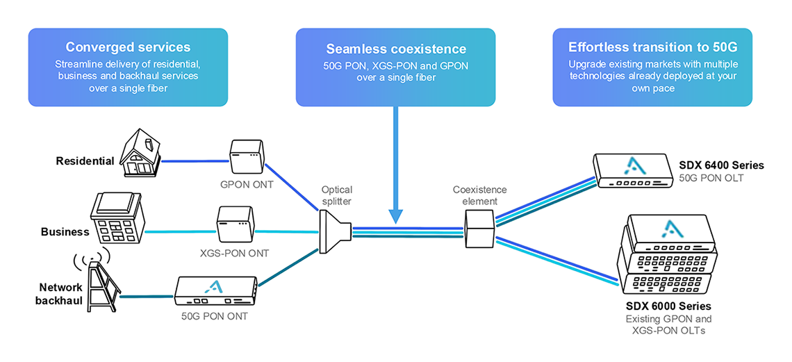
Image Credit: ADTRAN
…………………………………………………………………………………………………………………………………………………………………………………………………………………………..
In residential networks, traffic is expected to increasingly consist of short-duration, high-throughput bursts associated with edge processing, real-time analytics, and interactive services. A 50G PON gateway can accommodate these patterns by transmitting high-density payloads over sub-millisecond intervals, after which shared channel resources are rapidly released for other users. This behavior contributes to improved utilization efficiency on shared fiber infrastructure.
Low-latency and low-jitter performance are important for emerging application classes, including distributed AI inference, synchronized edge workloads, and multi-stream ultra-high-definition media. These requirements extend across both the access network and the in-home wireless domain, reinforcing the need for coordinated evolution of PON and Wi-Fi technologies.
From a deployment perspective, introduction of 50G-capable CPE provides operators with additional capacity headroom and supports alignment with future service requirements. Coupled with advancements in IEEE 802.11bn, this approach enables continued scaling of residential broadband performance while maintaining consistency across access and local network segments.
BCM68850 – 50G PON Edge AI Gateway SoC:
The BCM68850 is a standalone 50G PON Gateway SoC that provides an industry-standard ITU-T path for operators to future-proof their networks. The device features:
- High-Performance Application Engine: A dedicated CPU for third-party and operator applications leveraging industry available middleware.
- Integrated Neural Engine: A dedicated NPU that accelerates Edge AI inference, reducing cloud latency and enhancing data privacy by keeping sensitive information on premises.
- Symmetric 50G Performance: Delivers full 50G throughput to meet the insatiable appetite for reliable, multi-gigabit bandwidth.
- Wi-Fi 8 Ready: Native compatibility with Wi-Fi 8 standards to ensure the highest reliability and real-world consistency at the broadband edge.
- Intelligent Self-Healing: Enables operators to implement real-time anomaly detection and predictive bandwidth optimization, reducing OpEx and improving ARPU.
- Advanced Security: Incorporates enhanced security algorithms, including Post-Quantum Cryptography (PQC).
“The BCM68850 is a defining milestone for global fiber networks; we are reshaping the broadband edge as the central intelligence hub of the home,” said Philip Radtke, vice president of product marketing for Broadcom’s Wireless and Broadband Communications Division. “This flagship SoC joins our established lineup of NPU-accelerated fiber, cable, set-top box, and Wi-Fi solutions, ensuring operators can efficiently deploy edge-intelligent broadband regardless of the access medium and extend that intelligence all the way to the edge.”
“With ever increasing consumer and enterprise demand for bandwidth and ultra-reliable connectivity, operators are upgrading the Central Office and End Points with 50G PON capability. Next-generation solutions such as Broadcom’s BCM68850 SoC are critical to unlocking the value of this investment by future-proofing the network edge and ensuring high service levels at every node and premise,” said Jaimie Lenderman, practice leader for Optical, IP, and Broadband Infrastructure market research at Omdia.”By establishing a true end-to-end 50G pipe, operators can deliver the massive capacity and deterministic low latency required to support the rigors of the imminent Wi-Fi 8 deployment cycle.”
This end-to-end 50G offering completes the path from Broadcom’s BCM68660 OLT to the edge, providing a seamless and technically robust ecosystem comprising the BCM55050 ONT or the BCM68850 CPE gateway. This architecture introduces a new level of efficiency by optimizing CPU and memory resources for the AI era, ensuring that the home gateway can handle the massive data pipes required for the next decade of digital innovation.
About Broadcom:
Broadcom Inc. (NASDAQ: AVGO) is a technology leader that designs, develops, and supplies semiconductors and infrastructure software for global organizations’ complex, mission-critical needs. Broadcom combines long-term R&D investment with superb execution to deliver the best technology, at scale. Broadcom is a Delaware corporation headquartered in Palo Alto, CA. For more information, visit www.broadcom.com.
Broadcom, the pulse logo, and Connecting Everything are among the trademarks of Broadcom. The term “Broadcom” refers to Broadcom Inc., and/or its subsidiaries. Other trademarks are the property of their respective owners.
References:
https://www.broadcom.com/company/news/product-releases/64341
2026 Fiber Connect Keynote: “The Future of Fiber Optics: AI and the Quantum”
Nokia and Google Fiber trial 50G PON – first in the U.S.
HKT is first to deploy 50G PON technology in Hong Kong
Türk Telekom and ZTE trial 50G PON, but commercial deployment is not imminent
Ooredoo Qatar is first operator in the world to deploy 50G PON
Highlights of FiberConnect 2024: PON-related products dominate
Fiber Connect 2023: Telcos vs Cablecos; fiber symmetric speeds vs. DOCSIS 4.0?
Cisco’s Silicon One G300 as the dominant AI networking fabric, competing with Broadcom’s Tomahawk 6 series
On February 10, 2026, Cisco announced the Silicon One G300 102.4 Tbps Ethernet switch silicon, claiming it can power gigawatt-scale AI clusters for training, inference, and real-time agentic workloads, while maximizing GPU utilization with a 28% improvement in job completion time. The G300 was said to offer Intelligent Collective Networking, which combines an industry-leading fully shared packet buffer, path-based load balancing, and proactive network telemetry to offer better performance and profitability for large-scale data centers. It efficiently absorbs bursty AI traffic, responds faster to link failures, and prevents packet drops that can stall jobs, ensuring reliable data delivery even over long distances. With Intelligent Collective Networking, Cisco can deliver 33% increased network utilization, and a 28% reduction in job completion time versus simulated non-optimized path selection, making AI data centers more profitable with more tokens generated per GPU-hour. Also, the Cisco Silicon One G300 is highly programmable, enabling equipment to be upgraded for new network functionality even after it has been deployed. This enables Silicon One-based products to support emerging use cases and play multiple network roles, protecting long-term infrastructure investments. And with security fused into the hardware, customers can embrace holistic, at-speed security to keep clusters up and running.
The Cisco Silicon One G300 will power new Cisco N9000 and Cisco 8000 systems that push the frontier of AI networking in the data center. The systems feature innovative liquid cooling and support high-density optics to achieve new efficiency benchmarks and ensure customers get the most out of their GPU investments. In addition, the company enhanced Nexus One to make it easier for enterprises to operate their AI networks — on-premises or in the cloud — removing the complexity that can hold organizations back from scaling AI data centers.
“We are spearheading performance, manageability, and security in AI networking by innovating across the full stack – from silicon to systems and software,” said Jeetu Patel, President and Chief Product Officer, Cisco. “We’re building the foundation for the future of infrastructure, supporting every type of customer—from hyperscalers to enterprises—as they shift to AI-powered workloads.”
“As AI training and inference continues to scale, data movement is the key to efficient AI compute; the network becomes part of the compute itself. It’s not just about faster GPUs – the network must deliver scalable bandwidth and reliable, congestion-free data movement,” said Martin Lund, Executive Vice President of Cisco’s Common Hardware Group. “Cisco Silicon One G300, powering our new Cisco N9000 and Cisco 8000 systems, delivers high-performance, programmable, and deterministic networking – enabling every customer to fully utilize their compute and scale AI securely and reliably in production.”
The networking industry reaction to Cisco’s newest ASIC has been largely positive, with industry analysts and partners highlighting its role in reclaiming Cisco’s dominance in the AI infrastructure market. For example, Brendan Burke of Futurium thinks Cisco’s Silicon One G300 could be the backbone of Agentic AI Inference. His take: “Cisco’s latest announcements represent a calculated move to assert dominance in the AI networking fabric by attacking the specific bottlenecks of GPU cluster efficiency. As AI workloads shift toward agentic inference, where autonomous agents continuously interact across distributed environments, the network must handle unpredictable traffic patterns, unlike the structured flows of traditional training. Cisco is leveraging its vertical integration strategy to address the reliability and power constraints that plague these massive clusters. By emphasizing programmable silicon and rigorous optic qualification, Cisco aims to decouple network lifespan from rapid GPU innovation cycles, ensuring infrastructure can adapt to new traffic steering algorithms without hardware replacements. The G300 is a bid to make Ethernet the undisputed standard for AI back-end networks.”
- Industry-Leading Specs: Market analysts have noted that the G300’s 102.4 Tbps switching capacity sets a new benchmark for AI scale-out and scale-across networking.
- Efficiency Gains: Initial simulations showing a 28% reduction in job completion time (JCT) and a 33% increase in network utilization have been cited as major differentiators for large-scale AI clusters.
- Sustainability Focus: The shift toward liquid-cooled systems for the G300, which offers 70% greater energy efficiency per bit, is being viewed as a critical move for sustainable AI growth.
- Competitive Positioning: Experts from HyperFRAME Research suggest that the new silicon signals a “new confidence” from Cisco, positioning them as the “Apple of infrastructure” by tightly integrating hardware and software.
- AI Infrastructure Pivot: Financial analysts at Seeking Alpha have upgraded Cisco’s outlook, viewing the company no longer as just a legacy hardware firm but as a central player in the AI revolution.
- Partner Confidence: Major partners, such as Shanghai Lichan Technology, have expressed excitement about the Nexus 9100 Series powered by this silicon, specifically for its ability to simplify and scale AI deployments.
- Nvidia & Broadcom Competition: While the G300 is seen as a strong challenger to Nvidia’s Spectrum-X and Broadcom’s Tomahawk/Jericho lines, some observers note that Cisco still faces a steep climb to regain market share lost to these competitors in recent years.
- Complexity Concerns: Some industry veterans have pointed out that while the silicon is “hyperscale ready,” the success of these ASICs in the enterprise will depend on Cisco’s ability to maintain operational simplicity through tools like the Nexus Dashboard.
……………………………………………………………………………………………………………………………………………………………………………………………
|
Cisco Silicon One G300
|
Broadcom Tomahawk 6 (BCM78910 Series)
|
|---|---|
|
Bandwidth
102.4 Tbps  |
Bandwidth
102.4 Tbps  |
|
Manufacturing Process
TSMC 3nm  |
Manufacturing Process
3nm technology |
|
SerDes Lanes & Speed
512 lanes at 200 Gbps per link  |
SerDes Lanes & Speed
512 lanes at 200 Gbps per link, or 1024 lanes at 100G |
|
Port Configuration
Up to 64 x 1.6TbE ports or 512 x 200GbE ports |
Port Configuration
Up to 64 x 1.6TbE ports or 512 x 200GbE ports |
|
Target AI Cluster Size
Supports deployments of up to 128,000 GPUs |
Target AI Cluster Size
Supports over 100,000 XPUs (accelerators) Broadcom |
- Congestion Management: Cisco differentiates its G300 with an “Intelligent Collective Networking” approach featuring a fully shared packet buffer and a load-balancing agent that communicates across all G300s in the network to build a global map of congestion. Broadcom’s Tomahawk series also includes smart congestion control and global load balancing, though Cisco claims its implementation achieves higher network utilization (33% better).
- Programmability: Cisco emphasizes P4 programmability, allowing customers to update network functionality even after deployment.
- Ecosystem & Integration: Broadcom operates primarily in the merchant silicon market, with their chips used by various partners like HPE Juniper Networking. Cisco uses its own silicon to power its
Nexus 9000 and 8000 Series switches, tightly integrating hardware with software management platforms like Nexus One for a unified solution.
- Cooling Solutions: The Cisco G300 is designed to support high-density optics and is offered in new systems that include liquid-cooled options, providing 70% greater energy efficiency per bit compared to previous generations.
………………………………………………………………………………………………………………………………………………………………………………
References:
https://newsroom.cisco.com/c/r/newsroom/en/us/a/y2026/m02/cisco-announces-new-silicon-one-g300.html
https://blogs.cisco.com/sp/cisco-silicon-one-g300-the-next-wave-of-ai-innovation
Will Cisco’s Silicon One G300 Be the Backbone of Agentic Inference?
Analysis: Ethernet gains on InfiniBand in data center connectivity market; White Box/ODM vendors top choice for AI hyperscalers
Cisco CEO sees great potential in AI data center connectivity, silicon, optics, and optical systems
Networking chips and modules for AI data centers: Infiniband, Ultra Ethernet, Optical Connections
Nvidia enters Data Center Ethernet market with its Spectrum-X networking platform
Will AI clusters be interconnected via Infiniband or Ethernet: NVIDIA doesn’t care, but Broadcom sure does!
Research & Markets: WiFi 6E and WiFi 7 Chipset Market Report; Independent Analysis
According to Research & Markets, the WiFi 6E (IEEE 802.11ax) and WiFi 7 (IEEE 802.11be [1.]) chipset market is expanding rapidly, with projections indicating a rise from $33.65 billion in 2024 to $40.50 billion by 2025, and estimates reaching $149.65 billion by 2032. This growth reflects a notable CAGR of 20.50%, primarily driven by organizations upgrading their wireless networks in response to rising digital application use and increasing data volume.
Note 1. IEEE 802.11be standard was published July 22, 2025. The Project Approval Request (PAR) is here.
Enterprises today require scalable, secure wireless infrastructure capable of supporting diverse and demanding workloads. The latest WiFi chipsets improve network performance, facilitate secure operations, and support robust digital transformation strategies. Adopting Wi-Fi 6E and Wi-Fi 7 chipsets positions organizations to deliver secure, agile connectivity with higher speeds and lower latency.
- Application Areas: Automotive organizations implement advanced chipsets to support secure, reliable vehicle connectivity and enhance driver-assistance systems. In consumer electronics, manufacturers drive higher interactivity and seamless device experiences with updated wireless integration. Enterprises emphasize improved workforce mobility, while healthcare adopts secure, high-speed wireless for telemedicine and remote diagnostics. Industry operators deploy chipsets to enable robotics, automation, and smart manufacturing environments.
- End Users: Commercial enterprises in sectors such as hospitality, offices, and retail seek enhanced connectivity to increase operational efficiency and elevate customer engagement. Industrial segments-including utilities and manufacturing-prioritize automation and resilient communications infrastructure. Residential users focus on smart technology integration and flexible, connected home environments.
- Chipset Technologies: Integrated combo chips provide straightforward deployment for rapid delivery and compatibility, while discrete chipsets offer a tailored approach in high-volume or specialized scenarios. System-on-chip solutions bring high-density integration, maximizing energy efficiency and aligning with sustainability targets.
- Distribution Channels: Organizations maintain robust supply chains utilizing established resellers and digital platforms, ensuring prompt response to evolving logistical demands and market conditions.
- Regional Coverage: The Americas, Europe, Middle East and Africa, and Asia-Pacific each offer unique opportunities and regulatory landscapes, guiding deployment strategies and technology adoption in response to local dynamics.
- Company Profiles: The industry includes innovation-focused leaders such as Broadcom, Qualcomm, and MediaTek. These companies exhibit diverse approaches to integration and product differentiation across the competitive landscape.
Strategic Insights:
- The expanded wireless spectrum empowers businesses to scale connectivity, supporting data-rich operational environments where performance stability and capacity are critical.
- Next-generation chipset architectures enhance automation and real-time data management, particularly in healthcare and manufacturing, strengthening capabilities for time-sensitive applications.
- Collaborations between chipset vendors and device manufacturers improve compatibility, enabling tailored wireless infrastructure to address bespoke enterprise requirements.
- Maintaining a flexible supply approach-leveraging diverse distribution channels-supports organizational agility in facing evolving international trade and supply scenarios.
- Ongoing improvements in wireless security and system reliability support compliance and data protection needs for sectors operating under stringent regulatory requirements.
Market Insights:
- Surge in demand for Wi-Fi 7 chipsets optimized for multi-gigabit data throughput in dense public venues
- Integration of advanced OFDMA and multi-user MIMO enhancements to support simultaneous high-bandwidth applications
- Adoption of 6 GHz spectrum by enterprise networks to enable low-latency connectivity for critical IoT devices
- Development of energy-efficient chipset architectures to extend battery life in mobile and IoT applications
- Emergence of AI-driven adaptive beamforming techniques to improve signal reliability in complex environments
- Strategic partnerships between chipset vendors and cloud providers to accelerate edge computing deployments
- Certification focus on security enhancements such as WPA3-SAE to address evolving wireless threat vectors
- Custom chipset solutions for automotive and industrial automation requiring ultra-reliable low-latency performance
For more information about this report visit: https://www.researchandmarkets.com/r/q1rlgd
…………………………………………………………………………………………………………………………………
Independent Analysis:
The top three WiFi chipset vendors are:
- Broadcom Inc.: Broadcom is generally recognized as the market leader in the Wi-Fi 6/6E and Wi-Fi 7 segment, particularly in terms of revenue share. They supply chips for a wide range of devices, from high-performance consumer routers (e.g., Netgear, Asus models) to enterprise-grade networking equipment, and are a key supplier for platform upgrades like those in flagship smartphones.
- Qualcomm Technologies, Inc.: Qualcomm is a major competitor, especially in the mobile and networking infrastructure segments. Their “FastConnect 7800” chipset has positioned them for significant growth, with Wi-Fi 6E and 7 products expected to comprise a large portion of their Wi-Fi sales in 2025. They are also a primary chip provider for many high-end routers and mesh systems.
- MediaTek Inc.: MediaTek is a strong player, particularly in the consumer electronics space and in Asia-Pacific markets. Their “Filogic 380/880” Wi-Fi 7 chipsets have seen high demand, and they have strong partnerships with major brands like TP-Link and ZTE.
Other WiFi chipset vendors include: Marvell Technology Group, Intel, Realtek Semiconductor Corporation NXP Semiconductors, Texas Instruments, and Samsung Electronics Co. The market is competitive, with these vendors heavily investing in R&D and strategic partnerships to drive the adoption of new Wi-Fi standards from IEEE 802.11 WG.
The top markets for WiFi 6E/7 chipsets are: Smartphones, PC /laptops, Access Point/WiFi routers, CPE /gateways /extenders, industry verticals (e.g. manufacturing, automotive, industrial, home appliances, gaming, augmented reality, etc).
Sources: Gemini, Perplexity AI
……………………………………………………………………………………………………………………………………………………………………..
References:
https://www.ieee802.org/11/PARs/P802_11be_PAR_Detail.pdf
Wireless Broadband Alliance Report: WiFi 7, converged Wi-Fi and 5G, AI/Cognitive networks, and OpenRoaming
WiFi 7: Backgrounder and CES 2025 Announcements
WiFi 7 and the controversy over 6 GHz unlicensed vs licensed spectrum
MediaTek to expand chipset portfolio to include WiFi7, smart homes, STBs, telematics and IoT
MediaTek Announces Filogic Connectivity Family for WiFi 6/6E
Intel and Broadcom complete first Wi-Fi 7 cross-vendor demonstration with speeds over 5 Gbps
Qualcomm FastConnect 7800 combining WiFi 7 and Bluetooth in single chip
Rethink Research: Private 5G deployment will be faster than public 5G; WiFi 6E will also be successful
WBA field trial of Low Power Indoor Wi-Fi 6E with CableLabs, Intel and Asus
Aruba Introduces Industry’s 1st Enterprise-Grade Wi-Fi 6E Access Point
Custom AI Chips: Powering the next wave of Intelligent Computing
by the Indxx team of market researchers with Alan J Weissberger
The Market for AI Related Semiconductors:
Several market research firms and banks forecast that revenue from AI-related semiconductors will grow at about 18% annually over the next few years—five times faster than non-AI semiconductor market segments.
- IDC forecasts that global AI hardware spending, including chip demand, will grow at an annual rate of 18%.
- Morgan Stanley analysts predict that AI-related semiconductors will grow at an 18% annual rate for a specific company, Taiwan Semiconductor (TSMC).
- Infosys notes that data center semiconductor sales are projected to grow at an 18% CAGR.
- MarketResearch.biz and the IEEE IRDS predict an 18% annual growth rate for AI accelerator chips.
- Citi also forecasts aggregate chip sales for potential AI workloads to grow at a CAGR of 18% through 2030.
AI-focused chips are expected to represent nearly 20% of global semiconductor demand in 2025, contributing approximately $67 billion in revenue [1]. The global AI chip market is projected to reach $40.79 billion in 2025 [2.] and continue expanding rapidly toward $165 billion by 2030.

…………………………………………………………………………………………………………………………………………………
Types of AI Custom Chips:
Artificial intelligence is advancing at a speed that traditional computing hardware can no longer keep pace with. To meet the demands of massive AI models, lower latency, and higher computing efficiency, companies are increasingly turning to custom AI chips which are purpose-built processors optimized for neural networks, training, and inference workloads.
Those AI chips include Application Specific Integrated Circuits (ASICs) and Field- Programmable Gate Arrays (FPGAs) to Neural Processing Units (NPUs) and Google’s Tensor Processing Units (TPUs). They are optimized for core AI tasks like matrix multiplications and convolutions, delivering far higher performance-per-watt than CPUs or GPUs. This efficiency is key as AI workloads grow exponentially with the rise of Large Language Models (LLMs) and generative AI.
OpenAI – Broadcom Deal:
Perhaps the biggest custom AI chip design is being done by an OpenAI partnership with Broadcom in a multi-year, multi-billion dollar deal announced in October 2025. In this arrangement, OpenAI will design the hardware and Broadcom will develop custom chips to integrate AI model knowledge directly into the silicon for efficiency.
Here’s a summary of the partnership:
- OpenAI designs its own AI processors (GPUs) and systems, embedding its AI insights directly into the hardware. Broadcom develops and deploys these custom chips and the surrounding infrastructure, using its Ethernet networking solutions to scale the systems.
- Massive Scale: The agreement covers 10 gigawatts (GW) of AI compute, with deployments expected over four years, potentially extending to 2029.
- Cost Savings: This custom silicon strategy aims to significantly reduce costs compared to off-the-shelf Nvidia or AMD chips, potentially saving 30-40% on large-scale deployments.
- Strategic Goal: The collaboration allows OpenAI to build tailored hardware to meet the intense demands of developing frontier AI models and products, reducing reliance on other chip vendors.
AI Silicon Market Share of Key Players:
- Nvidia, with its extremely popular AI GPUs and CUDA software ecosystem., is expected to maintain its market leadership. It currently holds an estimated 86% share of the AI GPU market segment according to one source [2.]. Others put NVIDIA’s market AI chip market share between 80% and 92%.
- AMD holds a smaller, but growing, AI chip market share, with estimates placing its discrete GPU market share around 4% to 7% in early to mid-2025. AMD is projected to grow its AI chip division significantly, aiming for a double-digit share with products like the MI300X. In response to the extraordinary demand for advanced AI processors, AMD’s Chief Executive Officer, Dr. Lisa Su, presented a strategic initiative to the Board of Directors: to pivot the company’s core operational focus towards artificial intelligence. Ms. Su articulated the view that the “insatiable demand for compute” represented a sustained market trend. AMD’s strategic reorientation has yielded significant financial returns; AMD’s market capitalization has nearly quadrupled, surpassing $350 billion [1]. Furthermore, the company has successfully executed high-profile agreements, securing major contracts to provide cutting-edge silicon solutions to key industry players, including OpenAI and Oracle.
- Intel accounts for approximately 1% of the discrete GPU market share, but is focused on expanding its presence in the AI training accelerator market with its Gaudi 3 platform, where it aims for an 8.7% share by the end of 2025. The former microprocessor king has recently invested heavily in both its design and manufacturing businesses and is courting customers for its advanced data-center processors.
- Qualcomm, which is best known for designing chips for mobile devices and cars, announced in October that it would launch two new AI accelerator chips. The company said the new AI200 and AI250 are distinguished by their very high memory capabilities and energy efficiency.
Big Tech Custom AI chips vs Nvidia AI GPUs:
Big tech companies, including Google, Meta, Amazon, and Apple—are designing their own custom AI silicon to reduce costs, accelerate performance, and scale AI across industries. Yet nearly all rely on TSMC for manufacturing, thanks to its leadership in advanced chip fabrication technology [3.]
- Google recently announced Ironwood, its 7th-generation Tensor Processing Unit (TPU), a major AI chip for LLM training and inference, offering 4x the performance of its predecessor (Trillium) and massive scalability for demanding AI workloads like Gemini, challenging Nvidia’s dominance by efficiently powering complex AI at scale for Google Cloud and major partners like Meta. Ironwood is significantly faster, with claims of over 4x improvement in training and inference compared to the previous Trillium (6th gen) TPU. It allows for super-pods of up to 9,216 interconnected chips, enabling huge computational power for cutting-edge models. It’s optimized for high-volume, low-latency AI inference, handling complex thinking models and real-time chatbots efficiently.
- Meta is in advanced talks to purchase and rent large quantities of Google’s custom AI chips (TPUs), starting with cloud rentals in 2026 and moving to direct purchases for data centers in 2027, a significant move to diversify beyond Nvidia and challenge the AI hardware market. This multi-billion dollar deal could reshape AI infrastructure by giving Meta access to Google’s specialized silicon for workloads like AI model inference, signaling a major shift in big tech’s chip strategy, notes this TechRadar article.
- According to a Wall Street Journal report published on December 2, 2025, Amazon’s new Trainium3 custom AI chip presents a challenge to Nvidia’s market position by providing a more affordable option for AI development. Four times as fast as its previous generation of AI chips, Amazon said Trainium3 (produced by AWS’s Annapurna Labs custom-chip design business) can reduce the cost of training and operating AI models by up to 50% compared with systems that use equivalent graphics processing units, or GPUs. AWS acquired Israeli startup Annapurna Labs in 2015 and began designing chips to power AWS’s data-center servers, including network security chips, central processing units, and later its AI processor series, known as Inferentia and Trainium. “The main advantage at the end of the day is price performance,” said Ron Diamant, an AWS vice president and the chief architect of the Trainium chips. He added that his main goal is giving customers more options for different computing workloads. “I don’t see us trying to replace Nvidia,” Diamant said.
- Interestingly, many of the biggest buyers of Amazon’s chips are also Nvidia customers. Chief among them is Anthropic, which AWS said in late October is using more than one million Trainium2 chips to build and deploy its Claude AI model. Nvidia announced a month later that it was investing $10 billion in Anthropic as part of a massive deal to sell the AI firm computing power generated by its chips.

Image Credit: Emil Lendof/WSJ, iStock
Other AI Silicon Facts and Figures:
- Edge AI chips are forecast to reach $13.5 billion in 2025, driven by IoT and smartphone integration.
- AI accelerators based on ASIC designs are expected to grow by 34% year-over-year in 2025.
- Automotive AI chips are set to surpass $6.3 billion in 2025, thanks to advancements in autonomous driving.
- Google’s TPU v5p reached 30% faster matrix math throughput in benchmark tests.
- U.S.-based AI chip startups raised over $5.1 billion in venture capital in the first half of 2025 alone.
Conclusions:
Custom silicon is now essential for deploying AI in real-world applications such as automation, robotics, healthcare, finance, and mobility. As AI expands across every sector, these purpose-built chips are becoming the true backbone of modern computing—driving a hardware race that is just as important as advances in software. More and more AI firms are seeking to diversify their suppliers by buying chips and other hardware from companies other than Nvidia. Advantages like cost-effectiveness, specialization, lower power consumption and strategic independence that cloud providers gain from developing their own in-house AI silicon. By developing their own chips, hyperscalers can create a vertically integrated AI stack (hardware, software, and cloud services) optimized for their specific internal workloads and cloud platforms. This allows them to tailor performance precisely to their needs, potentially achieving better total cost of ownership (TCO) than general-purpose Nvidia GPUs
However, Nvidia is convinced it will retain a huge lead in selling AI silicon. In a post on X, Nvida wrote that it was “delighted by Google’s success with its TPUs,” before adding that Nvidia “is a generation ahead of the industry—it’s the only platform that runs every AI model and does it everywhere computing is done.” The company said its chips offer “greater performance, versatility, and fungibility” than more narrowly tailored custom chips made by Google and AWS.
The race is far from over, but we can expect to surely see more competition in the AI silicon arena.
………………………………………………………………………………………………………………………………………………………………………………….
Links for Notes:
2. https://sqmagazine.co.uk/ai-chip-statistics/
3. https://www.ibm.com/think/news/custom-chips-ai-future
References:
https://www.wsj.com/tech/ai/amazons-custom-chips-pose-another-threat-to-nvidia-8aa19f5b
https://www.wsj.com/tech/ai/nvidia-ai-chips-competitors-amd-broadcom-google-amazon-6729c65a
AI infrastructure spending boom: a path towards AGI or speculative bubble?
OpenAI and Broadcom in $10B deal to make custom AI chips
Reuters & Bloomberg: OpenAI to design “inference AI” chip with Broadcom and TSMC
RAN silicon rethink – from purpose built products & ASICs to general purpose processors or GPUs for vRAN & AI RAN
Dell’Oro: Analysis of the Nokia-NVIDIA-partnership on AI RAN
Cisco CEO sees great potential in AI data center connectivity, silicon, optics, and optical systems
Expose: AI is more than a bubble; it’s a data center debt bomb
China gaining on U.S. in AI technology arms race- silicon, models and research
OpenAI and Broadcom in $10B deal to make custom AI chips
Overview:
Late last October, IEEE Techblog reported that “OpenAI the maker of ChatGPT, was working with Broadcom to develop a new artificial intelligence (AI) chip focused on running AI models after they’ve been trained.” On Friday, the WSJ and FT (on-line subscriptions required) separately confirmed that OpenAI is working with Broadcom to develop custom AI chips, a move that could help alleviate the shortage of powerful processors needed to quickly train and release new versions of ChatGPT. OpenAI plans to use the new AI chip internally, according to one person close to the project, rather than make them available to external customers.
………………………………………………………………………………………………………………………………………………………………………………………….
Broadcom:
During its earnings call on Thursday, Broadcom’s CEO Hock Tan said that it had signed up an undisclosed fourth major AI developer as a custom AI chip customer, and that this new customer had committed to $10bn in orders. While Broadcom did not disclose the names of the new customer, people familiar with the matter confirmed OpenAI was the new client. Broadcom and OpenAI declined to comment, according to the FT. Tan said the deal had lifted the company’s growth prospects by bringing “immediate and fairly substantial demand,” shipping chips for that customer “pretty strongly” starting next year. “The addition of a fourth customer with immediate and fairly substantial demand really changes our thinking of what 2026 would be starting to look like,” Tan added.

Image credit: © Dado Ruvic/Reuters
HSBC analysts have recently noted that they expect to see a much higher growth rate from Broadcom’s custom chip business compared with Nvidia’s chip business in 2026. Nvidia continues to dominate the AI silicon market, with “hyperscalers” still representing the largest share of its customer base. While Nvidia doesn’t disclose specific customer names, recent filings show that a significant portion of their revenue comes from a small number of unidentified direct customers, which likely are large cloud providers like Microsoft, Amazon, Alphabet (Google), and Meta Platforms.
In August, Broadcom launched its Jericho networking chip, which is designed to help speed up AI computing by connecting data centers as far as 60 miles apart. By August, Broadcom’s market value had surpassed that of oil giant Saudi Aramco, making the chip firm the world’s seventh-largest publicly listed company.
……………………………………………………………………………………………………………………………………….
Open AI:
OpenAI CEO Sam Altman has been saying for months that a shortage of graphics processing units, or GPUs, has been slowing his company’s progress in releasing new versions of its flagship chatbot. In February, Altman wrote on X that ChatGPT-4.5, its then-newest large language model, was the closest the company had come to designing an AI model that behaved like a “thoughtful person,” but there were very high costs that came with developing it. “We will add tens of thousands of GPUs next week and roll it out to the plus tier then. (hundreds of thousands coming soon, and i’m pretty sure y’all will use every one we can rack up.)”
In recent years, OpenAI has relied heavily on so-called “off the shelf” GPUs produced by Nvidia, the biggest player in the chip-design space. But as demand from large AI firms looking to train increasingly sophisticated models has surged, chip makers and data-center operators have struggled to keep up. The company was one of the earliest customers for Nvidia’s AI chips and has since proven to be a voracious consumer of its AI silicon.
“If we’re talking about hyperscalers and gigantic AI factories, it’s very hard to get access to a high number of GPUs,” said Nikolay Filichkin, co-founder of Compute Labs, a startup that buys GPUs and offers investors a share in the rental income they produce. “It requires months of lead time and planning with the manufacturers.”
To solve this problem, OpenAI has been working with Broadcom for over a year to develop a custom chip for use in model training. Broadcom specializes in what it calls XPUs, a type of semiconductor that is designed with a particular application—such as training ChatGPT—in mind.
Last month, Altman said the company was prioritizing compute “in light of the increased demand from [OpenAI’s latest model] GPT-5” and planned to double its compute fleet “over the next 5 months.” OpenAI also recently struck a data-center deal with Oracle that calls for OpenAI to pay more than $30 billion a year to the cloud giant, and signed a smaller contract with Google earlier this year to alleviate computing shortages. It is also embarking on its own data-center construction project, Stargate, though that has gotten off to a slow start.
OpenAI’s move follows the strategy of tech giants such as Google, Amazon and Meta, which have designed their own specialized custom chips to run AI workloads. The industry has seen huge demand for the computing power to train and run AI models.
………………………………………………………………………………………………………………………………………………………………………………..
References:
https://www.ft.com/content/e8cc6d99-d06e-4e9b-a54f-29317fa68d6f
https://www.wsj.com/tech/ai/openai-broadcom-deal-ai-chips-5c7201d2
Reuters & Bloomberg: OpenAI to design “inference AI” chip with Broadcom and TSMC
Open AI raises $8.3B and is valued at $300B; AI speculative mania rivals Dot-com bubble
OpenAI announces new open weight, open source GPT models which Orange will deploy
OpenAI partners with G42 to build giant data center for Stargate UAE project
Generative AI Unicorns Rule the Startup Roost; OpenAI in the Spotlight
Networking chips and modules for AI data centers: Infiniband, Ultra Ethernet, Optical Connections
A growing portion of the billions of dollars being spent on AI data centers will go to the suppliers of networking chips, lasers, and switches that integrate thousands of GPUs and conventional micro-processors into a single AI computer cluster. AI can’t advance without advanced networks, says Nvidia’s networking chief Gilad Shainer. “The network is the most important element because it determines the way the data center will behave.”
Networking chips now account for just 5% to 10% of all AI chip spending, said Broadcom CEO Hock Tan. As the size of AI server clusters hits 500,000 or a million processors, Tan expects that networking will become 15% to 20% of a data center’s chip budget. A data center with a million or more processors will cost $100 billion to build.
The firms building the biggest AI clusters are the hyperscalers, led by Alphabet’s Google, Amazon.com, Facebook parent Meta Platforms, and Microsoft. Not far behind are Oracle, xAI, Alibaba Group Holding, and ByteDance. Earlier this month, Bloomberg reported that capex for those four hyperscalers would exceed $200 billion this year, making the year-over-year increase as much as 50%. Goldman Sachs estimates that AI data center spending will rise another 35% to 40% in 2025. Morgan Stanley expects Amazon and Microsoft to lead the pack with $96.4bn and $89.9bn of capex respectively, while Google and Meta will follow at $62.6bn and $52.3bn.
AI compute server architectures began scaling in recent years for two reasons.
1.] High end processor chips from Intel neared the end of speed gains made possible by shrinking a chip’s transistors.
2.] Computer scientists at companies such as Google and OpenAI built AI models that performed amazing feats by finding connections within large volumes of training material.
As the components of these “Large Language Models” (LLMs) grew to millions, billions, and then trillions, they began translating languages, doing college homework, handling customer support, and designing cancer drugs. But training an AI LLM is a huge task, as it calculates across billions of data points, rolls those results into new calculations, then repeats. Even with Nvidia accelerator chips to speed up those calculations, the workload has to be distributed across thousands of Nvidia processors and run for weeks.
To keep up with the distributed computing challenge, AI data centers all have two networks:
- The “front end” network which sends and receives data to/from external users —like the networks of every enterprise data center or cloud-computing center. It’s placed on the network’s outward-facing front end or boundary and typically includes equipment like high end routers, web servers, DNS servers, application servers, load balancers, firewalls, and other devices which connect to the public internet, IP-MPLS VPNs and private lines.
- A “back end” network that connects every AI processor (GPUs and conventional MPUs) and memory chip with every other processor within the AI data center. “It’s just a supercomputer made of many small processors,” says Ram Velaga, Broadcom’s chief of core switching silicon. “All of these processors have to talk to each other as if they are directly connected.” AI’s back-end networks need high bandwidth switches and network connections. Delays and congestion are expensive when each Nvidia compute node costs as much as $400,000. Idle processors waste money. Back-end networks carry huge volumes of data. When thousands of processors are exchanging results, the data crossing one of these networks in a second can equal all of the internet traffic in America.
Nvidia became one of today’s largest vendors of network gear via its acquisition of Israel based Mellanox in 2020 for $6.9 billion. CEO Jensen Huang and his colleagues realized early on that AI workloads would exceed a single box. They started using InfiniBand—a network designed for scientific supercomputers—supplied by Mellanox. InfiniBand became the standard for AI back-end networks.
While most AI dollars still go to Nvidia GPU accelerator chips, back-end networks are important enough that Nvidia has large networking sales. In the September quarter, those network sales grew 20%, to $3.1 billion. However, Ethernet is now challenging InfiniBand’s lock on AI networks. Fortunately for Nvidia, its Mellanox subsidiary also makes high speed Ethernet hardware modules. For example, xAI uses Nvidia Ethernet products in its record-size Colossus system.
While current versions of Ethernet lack InfiniBand’s tools for memory and traffic management, those are now being added in a version called Ultra Ethernet [1.]. Many hyperscalers think Ethernet will outperform InfiniBand, as clusters scale to hundreds of thousands of processors. Another attraction is that Ethernet has many competing suppliers. “All the largest guys—with an exception of Microsoft—have moved over to Ethernet,” says an anonymous network industry executive. “And even Microsoft has said that by summer of next year, they’ll move over to Ethernet, too.”
Note 1. Primary goals and mission of Ultra Ethernet Consortium (UEC): Deliver a complete architecture that optimizes Ethernet for high performance AI and HPC networking, exceeding the performance of today’s specialized technologies. UEC specifically focuses on functionality, performance, TCO, and developer and end-user friendliness, while minimizing changes to only those required and maintaining Ethernet interoperability. Additional goals: Improved bandwidth, latency, tail latency, and scale, matching tomorrow’s workloads and compute architectures. Backwards compatibility to widely-deployed APIs and definition of new APIs that are better optimized to future workloads and compute architectures.

……………………………………………………………………………………………………………………………………………………………………………………………………………………………….
Ethernet back-end networks offer a big opportunity for Arista Networks, which builds switches using Broadcom chips. In the past two years, AI data centers became an important business for Arista. AI provides sales to Arista switch rivals Cisco and Juniper Networks (soon to be a part of Hewlett Packard Enterprise), but those companies aren’t as established among hyperscalers. Analysts expect Arista to get more than $1 billion from AI sales next year and predict that the total market for back-end switches could reach $15 billion in a few years. Three of the five big hyperscale operators are using Arista Ethernet switches in back-end networks, and the other two are testing them. Arista CEO Jayshree Ullal (a former SCU EECS grad student of this author/x-adjunct Professor) says that back-end network sales seem to pull along more orders for front-end gear, too.
The network chips used for AI switching are feats of engineering that rival AI processor chips. Cisco makes its own custom Ethernet switching chips, but some 80% of the chips used in other Ethernet switches comes from Broadcom, with the rest supplied mainly by Marvell. These switch chips now move 51 terabits of data a second; it’s the same amount of data that a person would consume by watching videos for 200 days straight. Next year, switching speeds will double.
The other important parts of a network are connections between computing nodes and cables. As the processor count rises, connections increase at a faster rate. A 25,000-processor cluster needs 75,000 interconnects. A million processors will need 10 million interconnects. More of those connections will be fiber optic, instead of copper or coax. As networks speed up, copper’s reach shrinks. So, expanding clusters have to “scale-out” by linking their racks with optics. “Once you move beyond a few tens of thousand, or 100,000, processors, you cannot connect anything with copper—you have to connect them with optics,” Velaga says.
AI processing chips (GPUs) exchange data at about 10 times the rate of a general-purpose processor chip. Copper has been the preferred conduit because it’s reliable and requires no extra power. At current network speeds, copper works well at lengths of up to five meters. So, hyperscalers have tried to “scale-up” within copper’s reach by packing as many processors as they can within each shelf, and rack of shelves.
Back-end connections now run at 400 gigabits per second, which is equal to a day and half of video viewing. Broadcom’s Velaga says network speeds will rise to 800 gigabits in 2025, and 1.6 terabits in 2026.
Nvidia, Broadcom, and Marvell sell optical interface products, with Marvell enjoying a strong lead in 800-gigabit interconnects. A number of companies supply lasers for optical interconnects, including Coherent, Lumentum Holdings, Applied Optoelectronics, and Chinese vendors Innolight and Eoptolink. They will all battle for the AI data center over the next few years.
A 500,000-processor cluster needs at least 750 megawatts, enough to power 500,000 homes. When AI models scale to a million or more processors, they will require gigawatts of power and have to span more than one physical data center, says Velaga.
The opportunity for optical connections reaches beyond the AI data center. That’s because there isn’t enough power. In September, Marvell, Lumentum, and Coherent demonstrated optical links for data centers as far apart as 300 miles. Nvidia’s next-generation networks will be ready to run a single AI workload across remote locations.
Some worry that AI performance will stop improving as processor counts scale. Nvidia’s Jensen Huang dismissed those concerns on his last conference call, saying that clusters of 100,000 processors or more will just be table stakes with Nvidia’s next generation of chips. Broadcom’s Velaga says he is grateful: “Jensen (Nvidia CEO) has created this massive opportunity for all of us.”
References:
https://www.datacenterdynamics.com/en/news/morgan-stanley-hyperscaler-capex-to-reach-300bn-in-2025/
https://ultraethernet.org/ultra-ethernet-specification-update/
Will AI clusters be interconnected via Infiniband or Ethernet: NVIDIA doesn’t care, but Broadcom sure does!
Will billions of dollars big tech is spending on Gen AI data centers produce a decent ROI?
Canalys & Gartner: AI investments drive growth in cloud infrastructure spending
AI Echo Chamber: “Upstream AI” companies huge spending fuels profit growth for “Downstream AI” firms
AI wave stimulates big tech spending and strong profits, but for how long?
Markets and Markets: Global AI in Networks market worth $10.9 billion in 2024; projected to reach $46.8 billion by 2029
Using a distributed synchronized fabric for parallel computing workloads- Part I
Using a distributed synchronized fabric for parallel computing workloads- Part II
Reuters & Bloomberg: OpenAI to design “inference AI” chip with Broadcom and TSMC
Bloomberg reports that OpenAI, the fast-growing company behind ChatGPT, is working with Broadcom Inc. to develop a new artificial intelligence chip specifically focused on running AI models after they’ve been trained, according to two people familiar with the matter. The two companies are also consulting with Taiwan Semiconductor Manufacturing Company(TSMC) the world’s largest chip contract manufacturer. OpenAI has been planning a custom chip and working on its uses for the technology for around a year, the people said, but the discussions are still at an early stage. The company has assembled a chip design team of about 20 people, led by top engineers who have previously built Tensor Processing Units (TPUs) at Google, including Thomas Norrie and Richard Ho (head of hardware engineering).
Reuters reported on OpenAI’s ongoing talks with Broadcom and TSMC on Tuesday. It has been working for months with Broadcom to build its first AI chip focusing on inference (responds to user requests), according to sources. Demand right now is greater for training chips, but analysts have predicted the need for inference chips could surpass them as more AI applications are deployed.
OpenAI has examined a range of options to diversify chip supply and reduce costs. OpenAI considered building everything in-house and raising capital for an expensive plan to build a network of chip manufacturing factories known as “foundries.”
OpenAI may continue to research setting up its own network of foundries, or chip factories, one of the people said, but the startup has realized that working with partners on custom chips is a quicker, attainable path for now. Reuters earlier reported that OpenAI was pulling back from the effort of establishing its own chip manufacturing capacity. The company has dropped the ambitious foundry plans for now due to the costs and time needed to build a network, and plans instead to focus on in-house chip design efforts, according to sources.
OpenAI, which helped commercialize generative AI that produces human-like responses to queries, relies on substantial computing power to train and run its systems. As one of the largest purchasers of Nvidia’s graphics processing units (GPUs), OpenAI uses AI chips both to train models where the AI learns from data and for inference, applying AI to make predictions or decisions based on new information. Reuters previously reported on OpenAI’s chip design endeavors. The Information reported on talks with Broadcom and others.
The Information reported in June that Broadcom had discussed making an AI chip for OpenAI. As one of the largest buyers of chips, OpenAI’s decision to source from a diverse array of chipmakers while developing its customized chip could have broader tech sector implications.
Broadcom is the largest designer of application-specific integrated circuits (ASICs) — chips designed to fit a single purpose specified by the customer. The company’s biggest customer in this area is Alphabet Inc.’s Google. Broadcom also works with Meta Platforms Inc. and TikTok owner ByteDance Ltd.
When asked last month whether he has new customers for the business, given the huge demand for AI training, Broadcom Chief Executive Officer Hock Tan said that he will only add to his short list of customers when projects hit volume shipments. “It’s not an easy product to deploy for any customer, and so we do not consider proof of concepts as production volume,” he said during an earnings conference call.
OpenAI’s services require massive amounts of computing power to develop and run — with much of that coming from Nvidia chips. To meet the demand, the industry has been scrambling to find alternatives to Nvidia. That’s included embracing processors from Advanced Micro Devices Inc. and developing in-house versions.
OpenAI is also actively planning investments and partnerships in data centers, the eventual home for such AI chips. The startup’s leadership has pitched the U.S. government on the need for more massive data centers and CEO Sam Altman has sounded out global investors, including some in the Middle East, to finance the effort.
“It’s definitely a stretch,” OpenAI Chief Financial Officer Sarah Friar told Bloomberg Television on Monday. “Stretch from a capital perspective but also my own learning. Frankly we are all learning in this space: Infrastructure is destiny.”
Currently, Nvidia’s GPUs hold over 80% AI market share. But shortages and rising costs have led major customers like Microsoft, Meta, and now OpenAI, to explore in-house or external alternatives.
References:
AI Echo Chamber: “Upstream AI” companies huge spending fuels profit growth for “Downstream AI” firms
AI Frenzy Backgrounder; Review of AI Products and Services from Nvidia, Microsoft, Amazon, Google and Meta; Conclusions
AI sparks huge increase in U.S. energy consumption and is straining the power grid; transmission/distribution as a major problem
Generative AI Unicorns Rule the Startup Roost; OpenAI in the Spotlight
Will AI clusters be interconnected via Infiniband or Ethernet: NVIDIA doesn’t care, but Broadcom sure does!
InfiniBand, which has been used extensively for HPC interconnect, currently dominates AI networking accounting for about 90% of deployments. That is largely due to its very low latency and architecture that reduces packet loss, which is beneficial for AI training workloads. Packet loss slows AI training workloads, and they’re already expensive and time-consuming. This is probably why Microsoft chose to run InfiniBand when building out its data centers to support machine learning workloads. However, InfiniBand tends to lag Ethernet in terms of top speeds. Nvidia’s very latest Quantum InfiniBand switch tops out at 51.2 Tb/s with 400 Gb/s ports. By comparison, Ethernet switching hit 51.2 Tb/s nearly two years ago and can support 800 Gb/s port speeds.

While InfiniBand currently has the edge, several factors point to increased Ethernet adoption for AI clusters in the future. Recent innovations are addressing Ethernet’s shortcomings compared to InfiniBand:
- Lossless Ethernet technologies
- RDMA over Converged Ethernet (RoCE)
- Ultra Ethernet Consortium’s AI-focused specifications
Some real-world tests have shown Ethernet offering up to 10% improvement in job completion performance across all packet sizes compared to InfiniBand in complex AI training tasks. By 2028, it’s estimated that: 1] 45% of generative AI workloads will run on Ethernet (up from <20% now) and 2] 30% will run on InfiniBand (up from <20% now).
In a lively session at VM Ware-Broadcom’s Explore event, panelists were asked how to best network together the GPUs, and other data center infrastructure, needed to deliver AI. Broadcom’s Ram Velaga, SVP and GM of the Core Switching Group, was unequivocal: “Ethernet will be the technology to make this happen.” Velaga opening remarks asked the audience, “Think about…what is machine learning and how is that different from cloud computing?” Cloud computing, he said, is about driving utilization of CPUs; with ML, it’s the opposite.
“No one…machine learning workload can run on a single GPU…No single GPU can run an entire machine learning workload. You have to connect many GPUs together…so machine learning is a distributed computing problem. It’s actually the opposite of a cloud computing problem,” Velaga added.
Nvidia (which acquired Israel interconnect fabless chip maker Mellanox [1.] in 2019) says, “Infiniband provides dramatic leaps in performance to achieve faster time to discovery with less cost and complexity.” Velaga disagrees saying “InfiniBand is expensive, fragile and predicated on the faulty assumption that the physical infrastructure is lossless.”
Note 1. Mellanox specialized in switched fabrics for enterprise data centers and high performance computing, when high data rates and low latency are required such as in a computer cluster.
…………………………………………………………………………………………………………………………………………..
Ethernet, on the other hand, has been the subject of ongoing innovation and advancement since, he cited the following selling points:
- Pervasive deployment
- Open and standards-based
- Highest Remote Direct Access Memory (RDMA) performance for AI fabrics
- Lowest cost compared to proprietary tech
- Consistent across front-end, back-end, storage and management networks
- High availability, reliability and ease of use
- Broad silicon, hardware, software, automation, monitoring and debugging solutions from a large ecosystem
To that last point, Velaga said, “We steadfastly have been innovating in this world of Ethernet. When there’s so much competition, you have no choice but to innovate.” InfiniBand, he said, is “a road to nowhere.” It should be noted that Broadcom (which now owns VMWare) is the largest supplier of Ethernet switching chips for every part of a service provider network (see diagram below). Broadcom’s Jericho3-AI silicon, which can connect up to 32,000 GPU chips together, competes head-on with InfiniBand!
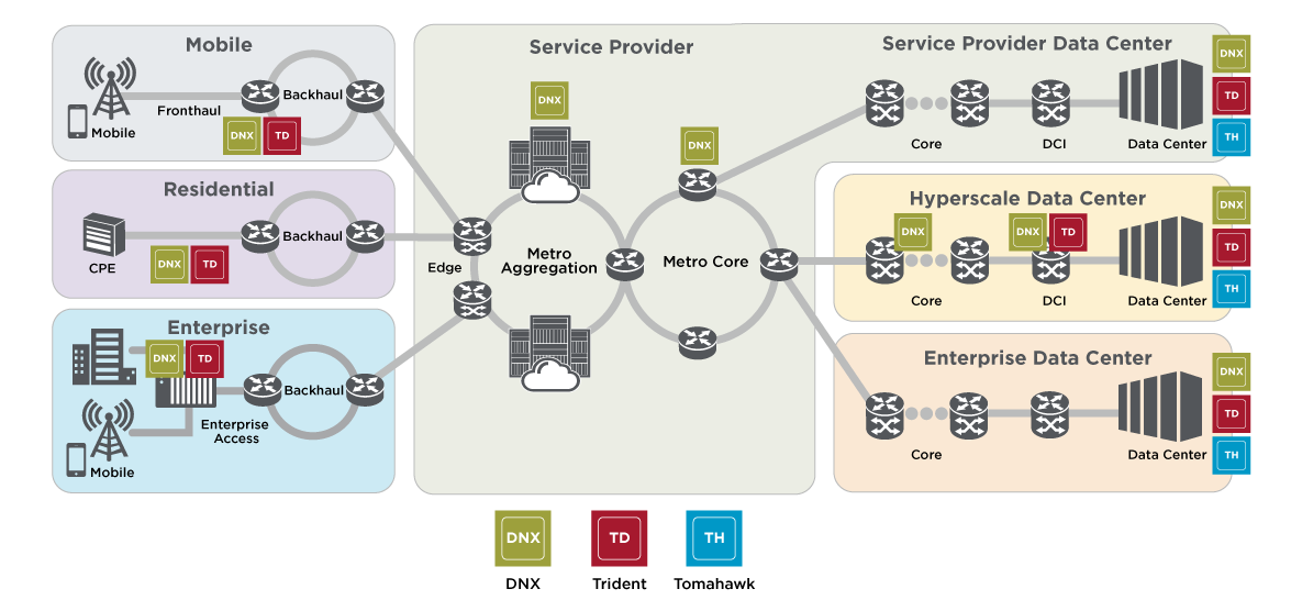
Image Courtesy of Broadcom
………………………………………………………………………………………………………………………………………………………..
Conclusions:
While InfiniBand currently dominates AI networking, Ethernet is rapidly evolving to meet AI workload demands. The future will likely see a mix of both technologies, with Ethernet gaining significant ground due to its improvements, cost-effectiveness, and widespread compatibility. Organizations will need to evaluate their specific needs, considering factors like performance requirements, existing infrastructure, and long-term scalability when choosing between InfiniBand and Ethernet for AI clusters.
–>Well, it turns out that Nvidia’s Mellanox division in Israel makes BOTH Infiniband AND Ethernet chips so they win either way!
…………………………………………………………………………………………………………………………………………………………………………..
References:
https://www.perplexity.ai/search/will-ai-clusters-run-on-infini-uCYEbRjeR9iKAYH75gz8ZA

https://www.theregister.com/2024/01/24/ai_networks_infiniband_vs_ethernet/
Broadcom on AI infrastructure networking—’Ethernet will be the technology to make this happen’
https://www.nvidia.com/en-us/networking/products/infiniband/h
ttps://www.nvidia.com/en-us/networking/products/ethernet/
Part1: Unleashing Network Potentials: Current State and Future Possibilities with AI/ML
Using a distributed synchronized fabric for parallel computing workloads- Part II
Part-2: Unleashing Network Potentials: Current State and Future Possibilities with AI/ML