

AI silicon
Google’s TPU Business Outpaces Rivals as Hyperscalers Accelerate Custom AI Silicon Strategies
Executive Summary:
Google parent Alphabet’s emerging business of selling artificial intelligence (AI) accelerator chips is twice as large as a cloud computing rival, Google executive Thomas Kurian claimed Tuesday at a Goldman Sachs investors conference.
On July 22, Google reported second-quarter cloud-computing revenue of $24.77 billion, up 82% year over year, driven by artificial intelligence workloads, handily beating estimates of $22.46 billion. For the first time, Google included third-party sales of AI accelerator chips, called tensor-processing units, in cloud revenue.
Kurian, head of Google’s cloud business, made these remarks at Goldman Sachs’ Communacopia conference:
“We offer the best computational infrastructure for AI, and we offer 3 types of silicon. NVIDIA GPUs, our own Tensor Processing Units (TPUs), custom ARM silicon. [As AI models generate code awe also offer our own Arm processors to run that code.] We offer 2.7x better price performance for training, 80% better price performance for inference, 30% better price performance for CPUs. All of that allows us to differentiate our portfolio from other providers. It allows us to offer solutions to financial markets and capital markets.”
“The size of our accelerator business, our TPU business, is more than twice that of the next-largest hyperscaler.”
“Our platform is called Gemini Enterprise. It is used by over 90% of the Fortune 100 and thousands of small businesses. It’s used in a very specific way. People want to use it as a reasoning agent. So break the plan, understand the steps that are needed, reason on it and execute the steps. So it uses a reasoning agent to understand all the information in the company to then automate that workflow process. And when it does it, you want strong controls. What kinds of controls? Companies are worried about security. They’re worried about auditing, what these agents are doing. They want to manage costs and set budget caps. We have all those controls. And we allow people to use the right model for the right task. So you don’t have to always use the most expensive model, saving people a lot of money in doing so. We have a range of companies from insurance.”
–>You can read the entire transcript here. For more on Google’s TPUs please see:
Will Google Cloud’s AI and data analytics revenue +TPU IP licensing income offset huge AI CAPEX to produce a decent ROI?
Google’s TPU photo
……………………………………………………………………………………………………………………………………………………
Kurian added that Google monetizes TPU systems through three business models. One is letting companies rent TPU processing at its own cloud business. Also, Google sells TPU systems directly for deployment in customers’ data centers. One such customer is Anthropic. Third, Google also sells TPUs through a Blackstone cloud computing joint venture.
Google’s AI Chip Business:
In May, Google introduced Ironwood, its eighth-generation of TPUs. The Ironwood TPUs target both training of AI models and “inferencing” — processing AI workloads.
In a report published Aug. 24, Morgan Stanley analyst Brian Nowak estimated that Google cloud could garner $84 billion in “first party” — meaning non-cloud rental — TPU sales in 2027.
“We are raising our TPU sale estimates to $27 billion selling at a 30% gross margin,” Nowak said. “In all, we now expect Google to sell 0.3 gigawatts of TPU systems in the second half of 2026, 3.2 gigawatts in 2027 and 4.2 gigawatts in 2028. This translates into $84 billion/$108 billion of TPU-related Google cloud revenue in 2027 and 2028.”
In Q2-2026, Google said its cloud computing order backlog jumped to $514 billion, up from $460 billion in Q1. The backlog is converted into realized revenue as new data centers come online and crunch artificial intelligence-related workloads — training AI models and processing AI apps.
Google has increased its 2026 capital spending guidance to a range of $195 billion to $205 billion. Most of the spendings is going toward AI data centers and AI model development. In Q2, capital spending jumped 100% from a year earlier to $44.9 billion.
Kurian, a former top executive at Oracle, took over as the cloud-computing unit’s CEO in November 2018. When Kurian arrived, Google’s cloud customers were mostly other tech companies. Under Kurian, Google has targeted enterprise customers with cloud-based data-analytics and artificial intelligence tools.
Hyperscaler Custom Silicon: Meta, Microsoft, Oracle, and the Shift to In-House AI Accelerators:
While Google’s TPU business has reached a scale that Kurian says is more than twice that of the next-largest hyperscaler, other cloud and platform operators are rapidly expanding their own custom AI silicon programs to reduce dependence on Nvidia GPUs and optimize cost, power, and workload-specific performance.
Amazon.com has developed in-house Trainium AI accelerators while Microsoft has developed Maia AI chips. Amazon is further ahead than Microsoft in selling AI chips to outside customers, analysts say.
Meta – MTIA Family Targets Inference at Scale:
Meta has moved aggressively into custom silicon with its Meta Training and Inference Accelerator (MTIA) family, announcing four new chips — MTIA 300, 400, 450, and 500 — in March 2026 as part of a strategy to diversify hardware sources and lower AI infrastructure costs. The MTIA 300 entered production in mid-2026, with subsequent generations rolling out on an approximately six-month cadence through 2027.
Meta’s MTIA chips are manufactured by TSMC and co-developed with Broadcom under a multi-year partnership extending through 2029. The roadmap spans ranking and recommendation training (MTIA 300), combined generative AI and ranking workloads (MTIA 400), and decode-optimized generative AI inference (MTIA 450 and 500), with mass deployment of the flagship MTIA 500 planned for late 2027. Meta plans to put its own AI chip into production in September and is aiming to roughly double the computing capacity across its data centres.
By mid-2026, Meta, Amazon, Microsoft, and OpenAI have each closed the gap on the three key AI inputs — custom chips, power, and models — that only Google held in 2021.
Microsoft: Maia 200 and the Push to External Customers:
Microsoft unveiled its first custom AI accelerator, Maia 100, at Hot Chips 2024, followed by the inference-optimized Maia 200 in January 2026. Maia 200, built on TSMC’s 3 nm process with more than 140 billion transistors, 216 GB of HBM3e, and over 10 PFLOPS of FP4 compute within a 750 W SoC TDP, is designed to deliver 30% better performance per dollar for AI token generation.blogs.
Maia 200 will serve multiple models, including OpenAI’s GPT-5.2, and support Microsoft Foundry, Microsoft 365 Copilot, and reinforcement learning workflows. Microsoft plans to unveil next-gen Maia 300 AI chip in September, aiming to lower costs for in-house and OpenAI models while actively courting major enterprise customers. Anthropic is reportedly in talks with Microsoft to rent the company’s custom AI server chips as it looks to expand computing capacity.blogs.
Oracle: Partner-Led AI Clusters Rather Than Custom Silicon:
Oracle has taken a different path, opting not to develop its own AI accelerator but instead building large-scale AI clusters using third-party chips from Nvidia and AMD. Oracle plans to install the first MI450-equipped Helios racks in its OCI data centers during the third quarter of 2026, with an initial deployment targeting 50,000 MI450 processors.
Oracle’s AI strategy emphasizes rapid deployment of massive GPU-based clusters to serve anchor tenants like OpenAI under a reported $300 billion, five-year cloud computing contract beginning in 2027. In parallel, OpenAI is diversifying its supply of compute by designing its own chips with partners like Broadcom, with the first custom AI inference chips expected to deploy in the second half of 2026.
Market Implications:
By 2026, five of six major AI players — Google, Meta, Amazon, Microsoft, and OpenAI — now control at least two of the three critical AI inputs (chips, power, models), down from only Google in 2021. This vertical integration trend is reshaping the AI infrastructure market, with hyperscalers increasingly using custom silicon to optimize cost and performance for specific workloads while maintaining strategic flexibility through multi-vendor GPU procurement.
Google’s TPU v7, Amazon’s Trainium 3, Microsoft’s Maia 2, and Meta’s MTIA 2 all ramped into volume production in 2025–2026, signaling a maturation of the hyperscaler custom silicon ecosystem. Meta is also the first commercial gigawatt AMD MI450 deployment in H2 2026, illustrating a hybrid approach that combines in-house accelerators with third-party GPUs.
…………………………………………………………………………………………………………………………………………………..
References:
https://www.investors.com/news/technology/google-stock-cloud-kurian-ai-chip-business/
Will Google Cloud’s AI and data analytics revenue +TPU IP licensing income offset huge AI CAPEX to produce a decent ROI?
Google announces Gemini: it’s most powerful AI model, powered by TPU chips
Google Cloud and Verizon Expand Strategic Partnership to Scale Enterprise AI and Autonomous Network Operations
AWS to deploy AI inference chips from Cerebras in its data centers; Anapurna Labs/Amazon in-house AI silicon products
Meta’s “Iris” AI Chip for MTIA: Implications for Telecom-Grade Optical Networking, DCI and High Capacity Ethernet Fabrics
Custom AI Chips: Powering the next wave of Intelligent Computing
AI Compute Has a Switchboard Problem: Orchestration & Data Center Fabric Explained
South Korean startup Rebellions to use open source software for carriers to quickly build AI stacks with its AI inferencing chips
Analysis: Nvidia–MediaTek Deepen AI Platform Collaboration -What it Means for AI RAN & DCI
Executive Summary:
Nvidia has expanded its partnership with Taiwan based semiconductor firm MediaTek, committing $3.5 billion to a bond investment the two companies describe as a deepening of their “longstanding collaboration to build the next generations of AI computing platforms.” The move extends Nvidia’s pattern of strategic capital deployment across its compute ecosystem, this time reaching into custom silicon and advanced packaging.
According to the announcement, the collaboration couples Nvidia’s accelerated computing, AI, graphics, and software stack with MediaTek’s capabilities in custom silicon, high-performance computing (HPC), system-on-chip (SoC) design, and advanced packaging. MediaTek vice chairman and CEO Rick Tsai framed the investment as reinforcing a relationship spanning “cloud AI infrastructure, local AI computing and automotive in the era of physical AI,” combining Nvidia’s accelerated-computing and AI software ecosystem with MediaTek’s AI technology portfolio and custom-silicon resources.
Over the past several years, MediaTek has repositioned itself from a supplier of predominantly mid- and low-tier handset chipsets into a presence across smartphones, AI data centers, automotive, and IoT. Securities firm Yuanta Financial Holdings expects the closer alignment to accelerate MediaTek’s transition from edge AI into data-center infrastructure, device-based AI computing, and automotive platforms. Trading in MediaTek shares was suspended on the Taipei exchange Tuesday after the stock hit its daily 10% upside limit. The shares closed at NT$4,315 (about US$136.05), reflecting investor enthusiasm for the deepening of the collaboration.
NVIDIA and MediaTek are collaborating in three major areas:
- AI infrastructure: MediaTek will work with NVIDIA’s NVLink Fusion ecosystem to enable customers to develop custom AI infrastructure designed to integrate with NVIDIA rack-scale systems and AI factories.
- Local AI computing: The companies will continue to collaborate on multiple generations of NVIDIA RTX Spark™ and DGX Spark™ PC chips, powering consumer PCs, AI developer supercomputers and enterprise-class workstations, that integrate NVIDIA GPUs with MediaTek SoCs.
- Automotive: MediaTek and NVIDIA will continue developing platforms for AI-powered, software-defined vehicles in the era of physical AI.
“AI is transforming every computing platform — from the world’s largest AI factories to the PC and the car,” said Jensen Huang, founder and CEO of NVIDIA. “MediaTek is one of the world’s great semiconductor companies, with exceptional expertise in system-on-chip design, connectivity, leading performance and power efficiency. Together, we’re building platforms that bring NVIDIA accelerated computing to new markets and give customers the freedom to create differentiated AI systems at enormous scale.”
“MediaTek and NVIDIA share a vision for making advanced AI computing pervasive across the technology landscape,” said Rick Tsai, vice chairman and CEO of MediaTek. “NVIDIA’s investment strengthens a collaboration that spans cloud AI infrastructure, local AI computing and automotive in the era of physical AI. By combining NVIDIA’s leadership in accelerated computing and AI software ecosystem with MediaTek’s expertise in a diverse AI technology portfolio from edge to cloud, and our leadership position in custom silicon, we can accelerate innovation for our customers.”
Custom AI Infrastructure and NVLink Fusion:
Yuanta identified MediaTek’s participation in Nvidia’s NVLink Fusion as the most consequential element of the arrangement. Through that linkage, MediaTek could support the design of custom AI chips for clients while connecting them directly into Nvidia’s AI infrastructure — a complementary rather than competing role alongside the GPU vendor’s proprietary interconnect fabric.
The scale of the bond purchase also signals Nvidia’s long-term commitment to the relationship. Nvidia, currently the world’s most valuable company at roughly a $5 trillion market capitalization, has been deploying capital aggressively across both upstream and downstream partners. This latest deal, however, inevitably risks overlapping with other Nvidia investments — notably its $2 billion partnership with Marvell, which is also heavily oriented around NVLink Fusion and pitch-for the RAN with a one-chip architecture.
NVLink Fusion vs. Ethernet Scale-Out Interconnect:
NVLink Fusion and Ethernet-based scale-out interconnects target fundamentally different layers of the AI fabric, and the distinction turns on memory semantics rather than raw link rate. NVLink Fusion sits in the scale-up domain: it delivers memory-coherent, tightly coupled attachment for custom XPUs into Nvidia’s rack-scale NVLink fabric, with point-to-point GPU/XPU-to-GPU/XPU connectivity and an integrated high-bandwidth-memory interface (NVHBM) that trades die area and power for latency and bandwidth. It is proprietary, closed, and full-coherency by design — precisely the properties that make it hard for open standards to clone. Ethernet scale-out, by contrast, is the scale-out workhorse governing traffic between racks, pods, and clusters; it is loss-based, coarser-grained, and standardized through Ultra Ethernet and the broader IEEE 802.3 ecosystem.
The real contest is not NVLink against Ethernet so much as how much of the memory-coherent scale-up domain Ethernet-based challengers can capture. Standards-backed alternatives — UALink 2.0, Ultra Ethernet, and Broadcom’s Scale-Up Ethernet (SUE) — are pressing into scale-up territory, but they lack NVLink’s memory coherency and direct XPU-to-XPU connectivity, and SUE explicitly does not wire GPUs directly to GPUs. Meanwhile Nvidia’s strategy with NVLink Fusion is to co-opt custom XPUs (AWS Trainium4, and now MediaTek- and Marvell-designed silicon) into its fabric rather than let them migrate to those open scale-up paths. The practical outcome in the data center is a layered model — Ethernet surging in scale-out, and NVLink Fusion consolidating the latency-sensitive, memory-coherent scale-up spine — with Nvidia working to keep its proprietary layer the mandatory gateway that custom accelerators must pass through to reach the wider Ethernet-based world.
The $3.5 billion convertible-bond investment is best read not as a portfolio decision but as a defensive move within the AI rack-scale interconnect stack. The technical centerpiece is MediaTek’s adoption of the NVLink Fusion platform. Nvidia positions it as the connectivity technology and intellectual property that lets hyperscalers and AI-native operators drop custom accelerators (“XPUs”) and CPUs directly into its NVLink scale-up fabric.
MediaTek will now build against the three subsystems that define NVLink Fusion: the NVLink Fusion chiplet, which bridges a customer’s custom XPU to the NVLink scale-up domain over photonic or electrical interconnects (the chiplet itself carries up to ~1.8 TB/s of bidirectional bandwidth); NVLink-C2C, the high-bandwidth die-to-die link between XPUs, Nvidia’s Vera/Rosa CPUs, and other compatible processors; and NVHBM, a customized high-bandwidth-memory interface that trades off die area and power efficiency. The strategic significance is that Nvidia is effectively licensing its interconnect and memory layer as a licensable subsystem rather than enforcing a closed, all-Nvidia island — which lets it absorb “frenemy” silicon into the fabric instead of fighting it.
Two implications stand out for interconnect strategy:
-
A hedge on hyperscaler in-house silicon. AWS has already integrated its Trainium4 custom ASICs with NVLink Fusion for rack-scale deployment, and Google, Meta, Microsoft, and OpenAI are all advancing private accelerators. By standardizing the interface (NVLink Fusion, NVLink-C2C, NVHBM, chiplets, and rack-scale integration) that these custom XPUs must speak, Nvidia keeps chiplets, packages, memory, and racks—the connective infrastructure itself—inside its own revenue funnel. MediaTek, in turn, becomes the design conduit that helps hyperscalers and frontier model firms get to that tape-out without building an independent scale-up stack.
-
The scale-up vs. scale-out contest sharpens. NVLink remains essentially the only mature, memory-coherent scale-up fabric in production, whereas Ethernet is consolidating its dominance in scale-out (front-end and increasingly AI back-end) fabrics, and standards like Ultra Ethernet, UALink, and Broadcom’s Scale-Up Ethernet (SUE) are pressing into the scale-up domain. UALink and SUE, notably, lack NVLink’s memory coherency and point-to-point GPU-to-GPU connectivity, so NVLink Fusion’s positioning — co-opting custom XPUs rather than competing with them — lowers the attack surface those open standards could otherwise exploit.
The buy-in therefore consolidates Nvidia’s grip on the two layers that are hardest to commoditize: the latency-sensitive scale-up interconnect and the custom-silicon design flow that feeds it. What operators and chip partners give up is architectural independence — the bond structure and NVLink Fusion licensing effectively bind MediaTek into Nvidia’s ecosystem rather than allowing it to become an independent AI data-center silicon house.
What It Means for AI-RAN:
For the RAN, this is arguably a more consequential signal than the data-center economics. Nvidia’s AI-RAN play, via the AI Aerial software-defined accelerated-computing platform and its founding role in the AI-RAN Alliance, is built on having vRAN and AI workloads share the same GPU-accelerated infrastructure — what the community variously calls “AI for RAN,” “AI on RAN,” and “AI-and-RAN” on common hardware.nvidia+1
Here the MediaTek deal intersects directly with Nvidia’s earlier $2 billion Marvell partnership, which last year wired Marvell into the same NVLink Fusion platform for both the AI factory and AI-RAN ecosystem — Marvell supplying custom XPUs and NVLink Fusion-compatible scale-up networking, while Nvidia contributes the Vera CPU, ConnectX NICs, BlueField DPUs, Spectrum-X switches, and the rack-scale AI compute. The two arrangements are complementary in practice but overlapping in intent: Marvell owns the scale-up networking and the “one-chip-to-rule-the-RAN” custom silicon angle, while MediaTek brings SoC design, advanced packaging, and stronger reach into edge, automotive, and device-grade silicon. Together they give Nvidia two design houses capable of producing custom XPUs that plug into both data-center racks and AI-RAN infrastructure.
The operative question for IEEE readers is whether this broadens the AI-RAN supplier base going forward. Ericsson and Samsung have indicated their vRAN software built for Intel could be ported to AMD or Arm silicon with relatively modest effort, and Dell’Oro projections already have AI-RAN taking a significant share of the broader RAN market. Nvidia’s strategy is to ensure that, however the RAN silicon shakes out, the scale-up fabric and the custom-XPU design path remain NVLink Fusion-based — extending its data-center interconnect franchise into the radio access domain itself. The risk, flagged in the news report, is over-concentration: stacking Marvell and MediaTek onto the same NVLink Fusion foundation concentrates architectural leverage in Nvidia’s hands and could crowd out the open, multi-vendor fabric choices that O-RAN advocates would prefer to see served by standard Ethernet and UALink-style paths.
References:
https://www.lightreading.com/finance/nvidia-tips-3-5b-into-mediatek-in-latest-tech-partnership
Analysis: Nvidia’s $2 billion investment in Marvell; NVLink Fusion ecosystem & RAN vendor silicon strategy
Ericsson and MediaTek Demonstrate 3GPP-Based GNSS RTK Positioning with Sub-30cm Accuracy Over a Commercial 5G Network
5G infrastructure moves from coverage and speeds to cloud-native, orchestration, automation and AI-assisted networks
MediaTek overtakes Qualcomm in 5G smartphone chip market
South Korean startup Rebellions to use open source software for carriers to quickly build AI stacks with its AI inferencing chips
South Korean chip startup Rebellions builds purpose-engineered Al accelerators to redefine energy-efficiency and scale in the age of large-scale Al. It aims to deliver the best performance per dollar per watt possible for inferencing and lower both capex and opex associated with running AI infrastructure. The company has been very selective about where it has established office locations and staffing: Korea, Japan, Singapore, Saudi Arabia and the United States.
Their flagship semiconductor product is the Rebel100, which uses a predictive, software-controlled DMA engine tightly coupled with an on-chip mesh to prefetch KV data proactively. This enbales 2.7TB/s effective bandwidth and reduces token-level latency in 32K+ context LLMs.
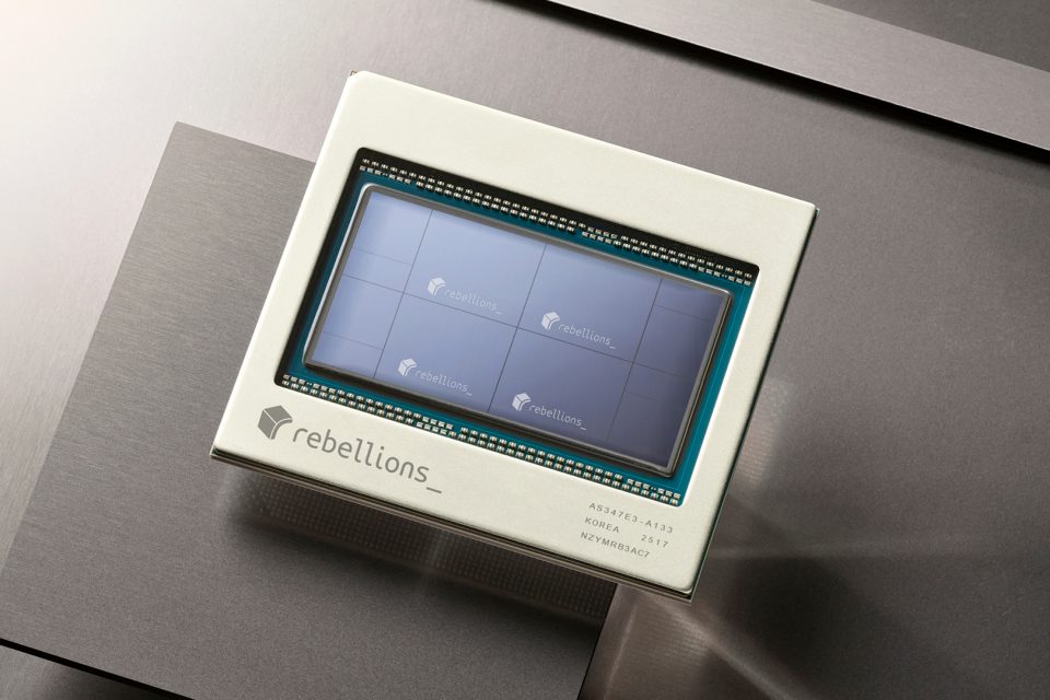
Image Credit: Rebellions
Gaining valuable experience in building an AI stack with SK Telecom, it’s pairing its field experience with an open source-first software strategy it said can help carriers move faster without locking scarce engineering talent into yet another proprietary AI stack. The company says it’s dedicated to using open-source software – everything from vLLM and OpenShift to PyTorch – with a “no forks” rule. The rule is designed to help customers avoid skills issues and ensure engineers don’t have to learn non-transferrable skills just to use its equipment.
Rebellions’ work with SK Telecom (SKT) has served as a foundational pillar of its engagement with other operators, according to Marshall Choy, Rebellions’ Chief Business Officer (CBO). The company is in conversations with between 10 and 20 operators around the world.
“Our systems have been deployed at SKT for nearly three years,” Choy said. “What does that mean? It means three years of lessons learned, institutional knowledge gain, product improvement and deep engagement with an end user customer working on real problems… It’s three years of blood sweat and tears that has become institutional knowledge,” he added.
The network operators in its pipeline are in “different stages of engagement and deployment” with Rebellions, Choy said, saying there will be “more to come on that.” While SK Telecom has been its most publicized partner to date, Choy said over the next 12 months Rebellions plans to highlight more of what has been going on under cover. That includes work with other telecom operators as well as neocloud operators, enterprises and governments.
According to Choy, the architecture prioritizes low-latency, high-throughput compute infrastructure. From a cost-efficiency perspective, the company targets a price-to-performance ratio that is two to three times more cost-effective than comparable Nvidia hardware. Furthermore, Rebellions delivers significantly higher energy efficiency. While an Nvidia DGX GB200 NVL72 system consumes upwards of 120 kilowatts per rack, Rebellions averages 4 kilowatts per system, or approximately 20 kilowatts per rack.
Choy noted that this power reduction yields a 6x savings in operational expenditure (OpEx). It also enables telecommunications providers to deploy Rebellions infrastructure in edge environments with stringent power constraints, such as legacy central offices. By retrofitting these distributed facilities with modern inference compute to serve LLM tokens, operators can maximize the lifecycle and return on investment (ROI) of their existing physical assets.
“Our goal is to reduce the unit economics of AI inferencing to near zero,” Choy said. While he admitted that sounds strange coming from an AI inferencing chip company, Choy explained that it’s all about making AI accessible for even more use cases – the ones where the math doesn’t work out today. “If you’re a telephone operator and you have an existing line card of services you provide, I can make you more profitable because I can lower your costs. But more strategically, what I can do is I can enable you to introduce a lower tier of services at a lower cost, which then makes AI inferencing accessible to a whole set of applications where it was previously too expensive,” he added.
It should be noted that Groq and SambaNova (see References below) are similarly working on chips to reduce the cost of inferencing. OpenAI appears to be moving in a similar direction with its Jalapeño chip.
Through its work with SK Telecom and others (unnamed), Choy said Rebellions has learned that customers aren’t just looking for hardware or software but for fully optimized infrastructure that cuts across both. That’s where Rebellions’ open-source ethos comes into play. “We didn’t want to have this mainframe model where everything is custom and bespoke and we’re this weird thing off in the side of the data center that doesn’t get touched by anything else,” Choy said. “It’s all about interoperability and integration.”
In conclusion, Choy opined, “Let’s be honest, the telcos don’t necessarily have all the right skills in place. So, being able to spread that across more of an open-source ecosystem means they can be in service and productive faster.”
References:
https://rebellions.ai/company/about/
https://rebellions.ai/category/blogs/
https://rebellions.ai/rebellions-product/rebel100/
SambaNova targets AI inference boom with chips built for existing data centers
Intel and AI chip startup SambaNova partner; SN50 AI inferencing chip max speed said to be 5X faster than competitive AI chips
AWS to deploy AI inference chips from Cerebras in its data centers; Anapurna Labs/Amazon in-house AI silicon products
Custom AI Chips: Powering the next wave of Intelligent Computing
Huawei to Double Output of Ascend AI chips in 2026; OpenAI orders HBM chips from SK Hynix & Samsung for Stargate UAE project
Huawei to Double Output of Ascend AI chips in 2026; OpenAI orders HBM chips from SK Hynix & Samsung for Stargate UAE project
Huawei to Double Output of Ascend AI chips in 2026; OpenAI orders HBM chips from SK Hynix & Samsung for Stargate UAE project
Superclusters of Nvidia GPU/AI chips combined with end-to-end network platforms to create next generation data centers