

AI Accelerator chips
Custom AI Silicon: OpenAI, Anthropic, Hyperscalers, Huawei and the Battle with Nvidia, AMD and Broadcom
Disclaimer: ChatGPT was used extensively to write this article.
Executive Summary:
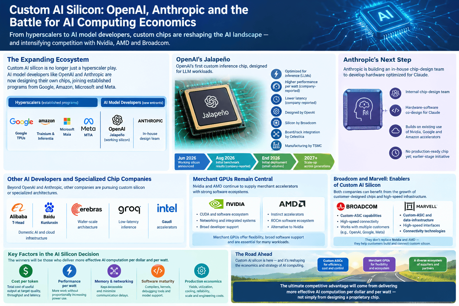
Custom AI silicon is entering a new phase. Google, Amazon, Microsoft and Meta have established proprietary accelerator programs, while OpenAI has introduced its first custom inference chip, Jalapeño, and Anthropic is assembling an in-house chip-design team.
These developments extend the industry trend examined in earlier IEEE Techblog articles, Custom AI Chips: Powering the Next Wave of Intelligent Computing and Google’s TPU Business Outpaces Rivals as Hyperscalers Accelerate Custom AI Silicon Strategies (see References for more).
The important new development is the entry of AI-model developers themselves into chip architecture and design. OpenAI is attempting to optimize hardware around the demands of its models and inference services, while Anthropic plans to pursue closer hardware-software co-design for Claude.
The competitive consequences extend beyond Nvidia and AMD. Broadcom and Marvell stand to benefit from demand for custom application-specific integrated circuits (ASICs), while Intel and specialized accelerator developers pursue alternative architectures.
The central question is whether custom silicon can deliver a sustained advantage in cost per AI token, energy efficiency and latency without sacrificing the flexibility and software ecosystem of merchant GPUs.
OpenAI – From Chip Partnership to Working Silicon:
OpenAI’s October 2025 agreement with Broadcom established a multiyear $10 billion custom-chip program for 10 gigawatts of OpenAI-designed accelerators and associated networking systems. Since then, the project has advanced from a development partnership to working silicon. On June 24, 2026, the companies unveiled Jalapeño, OpenAI’s first custom AI inference accelerator, designed specifically for large language models (LLMs). OpenAI designed the architecture, while Broadcom provides silicon implementation and networking expertise, and Celestica supports board and rack integration. TSMC will manufacture the chips. Engineering samples are running machine-learning workloads in the laboratory at targeted operating frequency and power. Initial deployment is planned for the end of 2026, followed by expansion over multiple generations.
In August 2026, OpenAI published initial benchmark results claiming substantial performance-per-watt and latency advantages over competing systems. These are company-reported results, not yet independent proof of a sustained production-scale advantage over Nvidia’s latest accelerators. Jalapeño is optimized for inference rather than general-purpose AI training, and OpenAI’s immediate priority is to meet its own rapidly growing computing demand.
The strategic significance is that OpenAI is extending its capabilities beyond AI models and software into custom hardware. By co-designing the chip, software kernels, memory movement, networking and serving systems, it aims to lower inference costs and improve responsiveness across ChatGPT, Codex and its API services. For Broadcom, the partnership reinforces the opportunity to supply custom silicon and networking technology to major AI developers without having to compete directly with Nvidia across the entire GPU market.
The distinction is significant: this is no longer simply a plan to develop proprietary silicon. OpenAI reported that engineering samples were running machine-learning workloads in its laboratories at production-target frequency and power.
Jalapeño is designed around large language model (LLM) inference rather than adapting a general-purpose GPU architecture. Its design emphasizes minimizing data movement and balancing compute, memory and networking resources. These considerations become increasingly important when serving interactive AI applications and agents that must generate responses quickly and execute multiple steps.
OpenAI designed the architecture, while Broadcom contributes silicon implementation and networking technology, and Celestica supports board and rack integration. OpenAI plans an initial deployment in small volumes near the end of 2026, with more substantial deployment expected in 2027.
The business rationale is straightforward. OpenAI operates ChatGPT, Codex and its API services at considerable computing scale. Even relatively modest improvements in inference efficiency could translate into meaningful savings if deployed across a large installed base.
However, Jalapeño’s initial benchmarks do not establish that it will outperform Nvidia’s latest systems across all workloads. Nor do they yet demonstrate its production-scale cost advantage. The relevant comparison must include complete systems, utilization, software development, power, cooling and operating costs.
The critical test is whether Jalapeño can deliver better economics at production scale. OpenAI must demonstrate that its claimed efficiency gains translate into lower total costs per AI token after accounting for manufacturing, memory, networking, power, cooling, utilization and software engineering. The initial results are promising, but the competitive outcome remains to be established.
Sources: OpenAI’s Jalapeño announcement and August benchmark results.
Author’s Note: The claims about Jalapeño’s performance are explicitly attributed to OpenAI.
……………………………………………………………………………………………………………………………………………
Anthropic – Building an Internal Design Capability:
Anthropic announced in August 2026 that it was forming an internal chip-design team to develop hardware optimized for Claude. The initiative reflects the same strategic logic as OpenAI’s: understanding a model’s architecture, inference patterns and software stack can help guide the design of more efficient processors.
Anthropic is not starting from a position of hardware independence. It already uses accelerators from Nvidia, Google and Amazon, among others. Its planned custom-silicon effort is an additional element of a multivendor strategy, not evidence that it is abandoning external suppliers.
The distinction between the two AI developers is important. OpenAI has demonstrated working silicon and published initial benchmarks; Anthropic is building a design organization and has not announced a production-ready proprietary accelerator or deployment timetable.
Designing advanced chips also requires substantial capital, specialized engineering talent and access to manufacturing and packaging capacity. Anthropic must ultimately demonstrate that the benefits justify those investments.
Source: Reuters on Anthropic’s chip-design team.
……………………………………………………………………………………………………………………………………………………..
Hyperscalers: Established Programs, Different Economics:
The major hyperscalers have already developed proprietary accelerators, as discussed in our September article. Their competitive positions differ according to the maturity of their hardware programs, their internal workloads and their ability to sell or rent computing capacity to external customers.
| Company | Custom silicon | Strategic emphasis |
|---|---|---|
| Tensor Processing Units (TPUs) | Training and inference, including external cloud customers | |
| Amazon | Trainium and Inferentia | AWS computing economics and customer choice |
| Microsoft | Maia | Azure AI inference and internal services |
| Meta | MTIA | Recommendation systems and generative AI inference |
| OpenAI | Jalapeño | LLM inference optimized around its models and serving software |
| Anthropic | In-house design initiative | Future hardware-software co-design for Claude |
Google’s position is particularly notable because it has an established TPU ecosystem and sells access to its accelerators beyond its own operations. Amazon similarly offers Trainium through AWS, giving customers an alternative to Nvidia-based infrastructure.
Microsoft and Meta are expanding their own programs, although proprietary silicon does not eliminate their need for merchant GPUs. Different workloads, development schedules and capacity requirements favor a mix of processors.
The broader point is that these companies are not necessarily trying to replace Nvidia everywhere. They are attempting to optimize selected workloads, diversify supply and improve the economics of operating AI infrastructure.
……………………………………………………………………………………………………………………………………………….
Huawei: Building an Alternative AI Silicon and Networking Ecosystem:
Huawei represents a different competitive challenge to NVIDIA, AMD and U.S. hyperscalers. Through its Ascend AI processors, HiSilicon semiconductor-design subsidiary, CANN software stack and high-speed interconnect technologies, Huawei is developing an integrated AI computing platform intended to reduce China’s dependence on foreign chips and software.
Huawei’s strategy extends beyond individual accelerators to cluster-scale infrastructure. Its September 2026 roadmap includes the Ascend 960DT, planned for the first quarter of 2027, and Ascend 960PR, planned for the third quarter 2026, followed by Ascend 970 and 980 generations in 2028 and 2029. Its UnifiedBus interconnect architecture is designed to connect processors, memory and storage across tightly coupled SuperPoD systems and larger AI clusters, potentially scaling to hundreds of thousands or even one million neural processing units (NPUs), according to Huawei’s announced architecture. These are roadmap and design targets, not independently verified production-scale performance results.
Manufacturing constraints: Huawei has also reported insufficient production capacity to meet domestic demand. That is a practical deployment constraint beyond the chip-design and software challenges.
Huawei’s principal challenge is translating this ambitious system architecture into competitive real-world performance. Advanced-chip manufacturing access, high-bandwidth memory (HBM) supply, power efficiency and the maturity of its CANN software ecosystem remain important constraints. NVIDIA benefits from a substantial lead in accelerator performance and a deeply established CUDA ecosystem, while AMD and hyperscalers pursue their own hardware and software strategies.
Nevertheless, Huawei is strategically significant because it combines AI silicon, interconnects, networking, storage and software within a broader computing and telecommunications portfolio. Its progress could reshape China’s domestic AI infrastructure market even if its chips do not match NVIDIA’s leading products on a per-accelerator basis. The competitive comparison must therefore consider total cluster performance, system availability, software compatibility, power consumption and cost—not chip specifications alone.
Huawei’s roadmap underscores a broader point: the AI-silicon competition is not simply a contest among chip designers. It is also a race to build complete, scalable computing platforms with the networking and software required to make thousands of accelerators work efficiently together.
Other AI Developers and Specialized Chip Companies:
The custom-silicon movement extends beyond OpenAI and Anthropic, but announced interest should not be confused with established production programs.
Alibaba’s T-Head and Baidu’s Kunlunxin are examples of Chinese semiconductor-development efforts associated with domestic AI and cloud infrastructure. Their importance includes reducing reliance on foreign suppliers amid restrictions on advanced semiconductor exports.
Among smaller AI-model developers, the strategic choices vary. A company can optimize models, compilers and kernels for existing processors without designing a chip of its own. Developing proprietary silicon becomes more attractive when workloads are large and predictable enough to justify substantial upfront investment.
Specialist chip companies pursue different alternatives to conventional GPUs:
- Cerebras uses a wafer-scale architecture designed to place substantial computing resources on a single silicon wafer.
- Groq developed a specialized architecture targeting low-latency inference and has entered a broader ecosystem that includes partnerships and technology integration.
- Intel offers its Gaudi accelerator family as an alternative AI-computing platform.
These vendors compete through different combinations of architecture, software, throughput, latency and system economics. They should not be treated as interchangeable with hyperscaler ASICs or general-purpose merchant GPUs.
……………………………………………………………………………………………………………………………………………..
Image from ChatGPT:
…………………………………………………………………………………………………………………………………………………………………………
Merchant Market AI Accelerator Chips from Nvidia and AMD :
Nvidia’s competitive advantage extends well beyond its GPU hardware. CUDA, optimized libraries, developer tools, networking and integrated rack-scale systems make its platform difficult to displace. Customers also benefit from a broad software ecosystem and the ability to use the same general platform across many workloads.
Nvidia’s vulnerability is that large AI operators have incentives to reduce costs and dependence on a single supplier. Custom ASICs can be attractive when workloads are sufficiently stable and deployment volumes justify specialized engineering.
AMD provides a second major merchant-GPU platform through its Instinct accelerators and ROCm software ecosystem. It offers customers another source of advanced computing capacity and an alternative to Nvidia’s platform.
AMD faces the challenge of expanding software adoption and competing against Nvidia’s established ecosystem. Nevertheless, the availability of multiple accelerator suppliers is strategically valuable to cloud providers and AI developers.
Neither company is likely to be displaced solely because a few major customers introduce proprietary chips. Merchant GPUs remain useful for new models, changing workloads and applications for which custom silicon is not yet economically justified.
Broadcom and Marvell – Beneficiaries of the Custom-ASIC Trend:
Broadcom occupies a particularly important position because it can benefit from the growth of customer-designed silicon without relying exclusively on sales of a proprietary general-purpose AI accelerator.
Its custom-ASIC capabilities, high-speed connectivity and networking products support the development of customer-specific AI systems. Its work with OpenAI and Meta illustrates how chip designers can retain control of their architectures while relying on semiconductor partners for implementation and infrastructure.
Marvell offers another set of custom-ASIC and data-infrastructure capabilities, including high-speed interfaces and connectivity technologies. It can benefit as companies develop specialized processors and build the systems needed to connect them.
The distinction from Nvidia and AMD is fundamental:
- Nvidia and AMD sell merchant accelerators to a broad customer base.
- Broadcom and Marvell help customers develop customized silicon and the associated data infrastructure.
- Hyperscalers and AI developers use their knowledge of workloads to decide where proprietary hardware can improve performance or economics.
These roles can overlap. Broadcom’s custom-chip business, for example, can benefit from a customer moving some workloads away from merchant GPUs. But custom silicon does not eliminate the need for advanced manufacturing, memory, packaging, networking or other semiconductor suppliers.
…………………………………………………………………………………………………………………………………………
What Will Determine the Winners?
The decisive metric is not peak computing performance alone. AI operators need to know how much useful work a complete system can deliver at an acceptable cost and latency.
Five factors will be especially important:
- Cost per token: Total cost of generating useful AI output at specified quality, throughput and response time.
- Performance per watt: The ability to serve more workloads without proportionally increasing electricity consumption.
- Memory and networking: The ability to keep model data accessible and minimize communication delays.
- Software maturity: The availability of compilers, optimized kernels, debugging tools and support for changing models.
- Production economics: Manufacturing yields, system utilization, cooling, reliability, deployment scale and engineering costs.
Custom ASICs are most compelling when a company has large, repeatable workloads and can optimize the model, software and hardware together. Merchant GPUs remain attractive when flexibility, rapid deployment and broad software support outweigh the potential benefits of specialization.
Power availability is an additional constraint. A more efficient processor can increase the useful computing capacity delivered by a given data-center power budget, although total electricity consumption may still rise as AI demand expands.
………………………………………………………………………………………………………………………………………
Conclusions:
Custom AI silicon is becoming a more important part of the industry’s computing strategy. The entry of OpenAI and Anthropic into chip design extends a trend already established by Google, Amazon, Microsoft and Meta.
OpenAI’s Jalapeño is a meaningful milestone because it has progressed from a partnership announcement to working silicon and published initial performance results. Anthropic’s initiative remains at an earlier stage. Both illustrate the growing interest in co-designing AI models, software and hardware.
The market is likely to remain heterogeneous. Nvidia and AMD will continue supplying merchant accelerators, while Broadcom and Marvell can benefit from demand for customer-specific silicon and high-speed networking. Specialized architectures will compete for workloads where their performance and cost advantages are compelling.
The ultimate competitive advantage will come from delivering more effective AI computation per dollar and per watt—not simply from designing a proprietary chip.
……………………………………………………………………………………………………………………………………
References:
Google’s TPU Business Outpaces Rivals as Hyperscalers Accelerate Custom AI Silicon Strategies
Custom AI Chips: Powering the next wave of Intelligent Computing
OpenAI and Broadcom in $10B deal to make custom AI chips
Meta’s “Iris” AI Chip for MTIA: Implications for Telecom-Grade Optical Networking, DCI and High Capacity Ethernet Fabrics
2026 OCP Summit: Full-Stack AI Networking Silicon from Nvidia/Cisco and Broadcom; Ethernet vs InfiniBand Interconnects
The AI Infrastructure Build-Out: A $10 Trillion Bet on Compute, Power, and Networks
Will Google Cloud’s AI and data analytics revenue +TPU IP licensing income offset huge AI CAPEX to produce a decent ROI?
Custom AI Silicon: OpenAI, Anthropic, Hyperscalers and the Battle with Nvidia, AMD and Broadcom
Microsoft Maia 300 Accelerator Chip: Co-Designing AI Inference for Improved Performance per Watt
Microsoft’s third-generation custom AI accelerator silicon (made by TSMC) combines a multi-process-node chiplet architecture with higher-density racks, targeting improved compute efficiency and lower infrastructure costs.
Executive Summary:
Microsoft announced its Maia 300 AI accelerator on October 12, 2026, outlining plans for multi-gigawatt deployments beginning in 2027. The company is positioning the third generation of its custom AI silicon as a key component of Azure’s infrastructure for inference workloads, including coding, long-context reasoning, and multi-step AI agent tasks.
Maia 300 reflects a broader shift in AI infrastructure design: optimizing the complete computing system rather than maximizing accelerator performance in isolation. Its chiplet architecture, high-bandwidth memory subsystem, and system-level integration are intended to improve throughput, power efficiency, and the economics of delivering AI services at scale.
Microsoft claims that Maia 300 delivers approximately 40% more tokens per megawatt than leading GPU-based systems. However, independent validation will require comparable workloads, clearly defined power boundaries, and measurements of throughput, latency, and output quality. The accelerator’s significance will ultimately depend on whether its architectural choices translate into lower costs per useful AI task under real-world operating conditions.

Azure Maia 200 now in production; Azure Maia 300 coming in 2027. Image credit: Microsoft
…………………………………………………………………………………………………………………………………………………………………………………………….
At a Glance- Key capabilities of the Maia 300 system:
Less data movement, more useful compute: Moving data efficiently, rather than raw compute power, is increasingly the bottleneck in large inference systems. Maia 300’s software-defined dataflow architecture and AI-assisted kernel optimization work together to maximize locality, reduce data movement and improve utilization across compute, memory and networking resources. By treating dataflow as a first-class design principle, Maia 300 delivers a significant performance-per-watt advantage over traditional GPU architectures.
Higher memory bandwidth within every watt: As AI workloads become increasingly context and memory-bound, Maia 300 delivers industry-leading HBM bandwidth per watt. Eight HBM4 stacks provide 18.0 TB/s of peak memory bandwidth within a 950-watt TDP, enabling efficient execution of large models and long-context workloads. Specialized kernel support uses on-die SRAM as a software-managed scratchpad, reducing pressure on HBM.
Chiplet architecture for enhanced efficiency: A new multi-chiplet architecture separates compute, memory-controller and I/O functions, improving efficiency, scalability and cost structure. Compute chiplets are built on TSMC’s N2P process node to maximize performance-per-watt.
Larger context, richer intelligence: By designing for advanced low-precision formats, including enhanced MXFP4, Maia 300 reduces memory and bandwidth requirements for both computation and KV-cache storage. The result is larger context windows, higher throughput and improved model efficiency within the same power envelope.
Scale-up networking at datacenter scale: Maia 300 treats networking as a seamless extension of the software-defined dataflow architecture. Rather than moving data through separate communication layers, dataflow operations span compute, memory and network resources as a single system. High-bandwidth interconnects between Maia accelerators are optimized for tensor parallelism, while a custom AI transport delivers performant and reliable scale-up communication across accelerators and racks. The AI-optimized transport leverages Ethernet-based networking infrastructure to enable a unified topology that scales efficiently from a single rack to datacenter-scale deployments.
Higher AI throughput from every rack: Maia 300 rack systems bring together 96 accelerators within a 167-kilowatt power envelope, delivering 27.6 TB of HBM capacity and 1.7 PB/s of aggregate HBM bandwidth across a high-speed scale-up domain. That density allows Microsoft to serve more simultaneous AI interactions and larger workloads from each rack, improving datacenter capacity and the economics of expanding AI services.
………………………………………………………………………………………………………………………………………………………………………………………….
Chiplet Architecture and Process Technology:
Maia 300 uses a chiplet architecture that partitions functions across multiple dies manufactured using different semiconductor process technologies. According to the reported design, the primary compute chiplets use TSMC’s advanced 2 nm-class technology, while other components use a 3 nm process. Other components, including those handling data movement between the processor and the rest of the system, use TSMC’s less expensive 3-nanometer process.
This approach differs from the Nvidia AI accelerator architecture described in the Reuters article, which combines a large central compute die with surrounding high-bandwidth memory chips. Microsoft’s design assigns different functions to different process nodes rather than manufacturing all components using the most advanced process.
This approach reflects an important principle in accelerator design: not every component benefits equally from the most advanced manufacturing process. Allocating compute-intensive functions to leading-edge technology while implementing other functions on different process nodes can improve manufacturing flexibility and potentially reduce overall costs.
However, process-node selection is only one aspect of the design. The performance of a chiplet-based accelerator also depends on die-to-die interconnect bandwidth, communication latency, packaging efficiency, power delivery, and thermal management. These factors determine how effectively the individual components operate as a unified processor.
For AI inference, this system-level perspective is particularly important. Increasing arithmetic throughput provides limited benefit when memory access or data movement becomes the dominant bottleneck. The architectural challenge is therefore to balance compute resources, memory bandwidth, and communication paths to sustain high utilization across representative workloads.
Memory Bandwidth and Inference Performance:
Memory architecture is central to the performance of large language model inference. Maia 300 incorporates eight high-bandwidth memory (HBM4) stacks, with Microsoft reporting peak memory bandwidth of 18.0 TB/s and a thermal design power of 950 W per accelerator.
These specifications provide useful indicators of the accelerator’s intended operating envelope, but peak bandwidth alone does not establish application performance. Actual results depend on memory access patterns, model architecture, batch size, sequence length, cache behavior, and the efficiency of the software stack.
Inference also encompasses distinct computational phases. During prompt processing, or prefill, accelerators process input tokens and may be constrained primarily by compute throughput. During autoregressive token generation, or decode, performance can become more sensitive to memory bandwidth, model-weight movement, and the size of the key-value (KV) cache used to retain context.
Long-context reasoning and agentic workloads introduce additional demands on memory capacity, data movement, and repeated model execution. Consequently, evaluating Maia 300 requires more than peak compute specifications: it requires sustained measurements across realistic inference workloads, including both throughput and latency.
Microsoft’s emphasis on inference-oriented design is therefore significant. The practical advantage will depend on how effectively the architecture converts available compute and memory resources into useful output tokens while meeting application-level latency requirements.
Rack Density, Power, and System-Level Efficiency:
Microsoft plans to deploy Maia 300 in racks containing 96 accelerators, with reported power consumption of approximately 167 kW per rack. For comparison, Nvidia’s GB300 rack configuration has been reported to contain 72 GPUs and consume approximately 142 kW. These figures illustrate the increasing power density of AI infrastructure, but they do not establish comparative performance or energy efficiency. Accelerator counts, rack configurations, and power measurements must be interpreted in the context of the complete system, including memory, networking, power conversion, and cooling.
Dividing reported rack power by accelerator count yields approximately 1.74 kW per Maia 300 accelerator position and 1.97 kW per GB300 GPU position. These are normalized rack-level figures, not measurements of individual accelerator power consumption. Differences in system configuration and measurement boundaries also limit their value as a direct comparison.
Microsoft separately claims that Maia 300 delivers approximately 40% more tokens per megawatt than leading GPU-based systems. This is a potentially important improvement because energy consumption is a major component of the cost of operating large-scale AI infrastructure. Nevertheless, the claim cannot be evaluated rigorously without identifying the comparison systems, workloads, software configurations, and power boundaries.
“It’s basically delivering more intelligence for every watt, every dollar, and every byte of memory by optimizing across the entire system,” Rani Borkar, president of Azure hardware systems and infrastructure at Microsoft, told Reuters.
A meaningful comparison should report aggregate token throughput alongside time to first token, inter-token latency, and sustained utilization. It should also distinguish accelerator or rack power from total facility power, which includes cooling and other datacenter overheads.
Ultimately, the relevant metric is not simply how many accelerators fit into a rack or how much power each rack consumes. It is how much useful inference work the complete system delivers for a given energy budget, while satisfying latency and quality requirements.
Hardware–Software Co-Design and Infrastructure Economics:
Custom AI silicon gives Microsoft greater control over the interaction between accelerator architecture, inference software, networking, and Azure’s datacenter infrastructure. This control can enable workload-specific optimization, improved resource utilization, and greater flexibility in deploying models across different hardware platforms.
However, custom silicon does not automatically produce lower costs. Its economics depend on manufacturing yields, packaging costs, software maturity, deployment scale, utilization, and the engineering effort required to optimize models and inference runtimes. Hardware specialization can also introduce trade-offs in flexibility as models and workloads evolve.
Microsoft’s reported plans for Maia 300 deployments spanning multiple gigawatts beginning in 2027 indicate the scale at which these considerations become important. The company also expects capital expenditures to exceed $175 billion in calendar year 2026, reflecting a broader investment in AI infrastructure rather than spending attributable solely to Maia 300.
At this scale, small improvements in sustained throughput per watt can have substantial operational consequences. Higher throughput may increase service capacity within a fixed power envelope, while lower energy consumption per token may reduce operating costs. Yet the financial benefit depends on actual utilization, workload mix, hardware lifecycle, and the total cost of operating the infrastructure.
The strategic objective is therefore broader than reducing dependence on third-party accelerators. It is to improve control over the cost, capacity, and performance of AI services through coordinated hardware and software design.
Deployment Scale and Validation Challenges:
Microsoft’s planned Maia 300 deployment raises several engineering questions that cannot be resolved by specifications alone.
First, how does the accelerator perform across different model sizes, context lengths, and inference patterns? Second, can its reported efficiency advantage be sustained under production concurrency and latency constraints? Third, how do networking, memory utilization, and software optimization affect performance when hundreds or thousands of accelerators operate as part of a larger service?
Independent evaluation should compare Maia 300 against clearly identified competing systems using equivalent models, output-quality requirements, precision settings, and inference software configurations. Measurements should include tokens per second, time to first token, inter-token latency, energy per generated token, and cost per million tokens. Agentic workloads may additionally require cost and latency measurements per successfully completed task.
These results should be reported with explicit power boundaries and sufficient methodological detail to permit reproduction. Without such evidence, peak specifications and vendor-reported efficiency figures remain useful indicators of design objectives, but not definitive proof of superior system performance.
Conclusions:
Microsoft Maia 300 illustrates how AI accelerator development is moving beyond the pursuit of peak compute performance toward system-level optimization. Its chiplet architecture, HBM4 memory subsystem, and integration with Azure’s inference infrastructure reflect the importance of balancing computation, memory bandwidth, data movement, and power consumption.
The central question is whether these architectural choices deliver sustained improvements in useful inference throughput, latency, and cost under real production conditions. Microsoft’s reported 40% advantage in tokens per megawatt is a promising claim, but its significance depends on transparent and comparable measurements.
As AI deployments grow, the competitive advantage of custom silicon will increasingly be determined by the efficiency of the complete system—not the specifications of the accelerator alone. Maia 300’s long-term importance will depend on whether Microsoft can translate hardware–software co-design into measurable gains in service capacity, energy efficiency, and the cost of delivering useful AI results.
…………………………………………………………………………………………………………………………………………………………………………………………………………………………………………..
References:
Reuters, “Microsoft plans huge deployment of its own AI chips, with an eye on saving costs,” Oct. 12, 2026.
Microsoft, official Maia 300 announcement and technical architecture materials, Oct. 12, 2026.
Nvidia, GB300 rack architecture and system power specifications. Cite the specific product documentation used to establish the 72-GPU configuration and 142 kW power figure.
TSMC, semiconductor process technology documentation. Cite the relevant process-node documentation to substantiate the manufacturing-node assignments reported for Maia 300.
Google’s TPU Business Outpaces Rivals as Hyperscalers Accelerate Custom AI Silicon Strategies
AWS to deploy AI inference chips from Cerebras in its data centers; Anapurna Labs/Amazon in-house AI silicon products
Huawei’s Ascend Silicon Roadmap Extends From AI Chips to Cluster-Scale Infrastructure
Custom AI Chips: Powering the next wave of Intelligent Computing
The AI Infrastructure Build-Out: A $10 Trillion Bet on Compute, Power, and Networks
Analysis: Nvidia–MediaTek Deepen AI Platform Collaboration -What it Means for AI RAN & DCI
Will Google Cloud’s AI and data analytics revenue +TPU IP licensing income offset huge AI CAPEX to produce a decent ROI?