

Month: September 2026
Google’s TPU Business Outpaces Rivals as Hyperscalers Accelerate Custom AI Silicon Strategies
Executive Summary:
Google parent Alphabet’s emerging business of selling artificial intelligence (AI) accelerator chips is twice as large as a cloud computing rival, Google executive Thomas Kurian claimed Tuesday at a Goldman Sachs investors conference.
On July 22, Google reported second-quarter cloud-computing revenue of $24.77 billion, up 82% year over year, driven by artificial intelligence workloads, handily beating estimates of $22.46 billion. For the first time, Google included third-party sales of AI accelerator chips, called tensor-processing units, in cloud revenue.
Kurian, head of Google’s cloud business, made these remarks at Goldman Sachs’ Communacopia conference:
“We offer the best computational infrastructure for AI, and we offer 3 types of silicon. NVIDIA GPUs, our own Tensor Processing Units (TPUs), custom ARM silicon. [As AI models generate code awe also offer our own Arm processors to run that code.] We offer 2.7x better price performance for training, 80% better price performance for inference, 30% better price performance for CPUs. All of that allows us to differentiate our portfolio from other providers. It allows us to offer solutions to financial markets and capital markets.”
“The size of our accelerator business, our TPU business, is more than twice that of the next-largest hyperscaler.”
“Our platform is called Gemini Enterprise. It is used by over 90% of the Fortune 100 and thousands of small businesses. It’s used in a very specific way. People want to use it as a reasoning agent. So break the plan, understand the steps that are needed, reason on it and execute the steps. So it uses a reasoning agent to understand all the information in the company to then automate that workflow process. And when it does it, you want strong controls. What kinds of controls? Companies are worried about security. They’re worried about auditing, what these agents are doing. They want to manage costs and set budget caps. We have all those controls. And we allow people to use the right model for the right task. So you don’t have to always use the most expensive model, saving people a lot of money in doing so. We have a range of companies from insurance.”
–>You can read the entire transcript here. For more on Google’s TPUs please see:
Will Google Cloud’s AI and data analytics revenue +TPU IP licensing income offset huge AI CAPEX to produce a decent ROI?
Google’s TPU photo
……………………………………………………………………………………………………………………………………………………
Kurian added that Google monetizes TPU systems through three business models. One is letting companies rent TPU processing at its own cloud business. Also, Google sells TPU systems directly for deployment in customers’ data centers. One such customer is Anthropic. Third, Google also sells TPUs through a Blackstone cloud computing joint venture.
Google’s AI Chip Business:
In May, Google introduced Ironwood, its eighth-generation of TPUs. The Ironwood TPUs target both training of AI models and “inferencing” — processing AI workloads.
In a report published Aug. 24, Morgan Stanley analyst Brian Nowak estimated that Google cloud could garner $84 billion in “first party” — meaning non-cloud rental — TPU sales in 2027.
“We are raising our TPU sale estimates to $27 billion selling at a 30% gross margin,” Nowak said. “In all, we now expect Google to sell 0.3 gigawatts of TPU systems in the second half of 2026, 3.2 gigawatts in 2027 and 4.2 gigawatts in 2028. This translates into $84 billion/$108 billion of TPU-related Google cloud revenue in 2027 and 2028.”
In Q2-2026, Google said its cloud computing order backlog jumped to $514 billion, up from $460 billion in Q1. The backlog is converted into realized revenue as new data centers come online and crunch artificial intelligence-related workloads — training AI models and processing AI apps.
Google has increased its 2026 capital spending guidance to a range of $195 billion to $205 billion. Most of the spendings is going toward AI data centers and AI model development. In Q2, capital spending jumped 100% from a year earlier to $44.9 billion.
Kurian, a former top executive at Oracle, took over as the cloud-computing unit’s CEO in November 2018. When Kurian arrived, Google’s cloud customers were mostly other tech companies. Under Kurian, Google has targeted enterprise customers with cloud-based data-analytics and artificial intelligence tools.
Hyperscaler Custom Silicon: Meta, Microsoft, Oracle, and the Shift to In-House AI Accelerators:
While Google’s TPU business has reached a scale that Kurian says is more than twice that of the next-largest hyperscaler, other cloud and platform operators are rapidly expanding their own custom AI silicon programs to reduce dependence on Nvidia GPUs and optimize cost, power, and workload-specific performance.
Amazon.com has developed in-house Trainium AI accelerators while Microsoft has developed Maia AI chips. Amazon is further ahead than Microsoft in selling AI chips to outside customers, analysts say.
Meta – MTIA Family Targets Inference at Scale:
Meta has moved aggressively into custom silicon with its Meta Training and Inference Accelerator (MTIA) family, announcing four new chips — MTIA 300, 400, 450, and 500 — in March 2026 as part of a strategy to diversify hardware sources and lower AI infrastructure costs. The MTIA 300 entered production in mid-2026, with subsequent generations rolling out on an approximately six-month cadence through 2027.
Meta’s MTIA chips are manufactured by TSMC and co-developed with Broadcom under a multi-year partnership extending through 2029. The roadmap spans ranking and recommendation training (MTIA 300), combined generative AI and ranking workloads (MTIA 400), and decode-optimized generative AI inference (MTIA 450 and 500), with mass deployment of the flagship MTIA 500 planned for late 2027. Meta plans to put its own AI chip into production in September and is aiming to roughly double the computing capacity across its data centres.
By mid-2026, Meta, Amazon, Microsoft, and OpenAI have each closed the gap on the three key AI inputs — custom chips, power, and models — that only Google held in 2021.
Microsoft: Maia 200 and the Push to External Customers:
Microsoft unveiled its first custom AI accelerator, Maia 100, at Hot Chips 2024, followed by the inference-optimized Maia 200 in January 2026. Maia 200, built on TSMC’s 3 nm process with more than 140 billion transistors, 216 GB of HBM3e, and over 10 PFLOPS of FP4 compute within a 750 W SoC TDP, is designed to deliver 30% better performance per dollar for AI token generation.blogs.
Maia 200 will serve multiple models, including OpenAI’s GPT-5.2, and support Microsoft Foundry, Microsoft 365 Copilot, and reinforcement learning workflows. Microsoft plans to unveil next-gen Maia 300 AI chip in September, aiming to lower costs for in-house and OpenAI models while actively courting major enterprise customers. Anthropic is reportedly in talks with Microsoft to rent the company’s custom AI server chips as it looks to expand computing capacity.blogs.
Oracle: Partner-Led AI Clusters Rather Than Custom Silicon:
Oracle has taken a different path, opting not to develop its own AI accelerator but instead building large-scale AI clusters using third-party chips from Nvidia and AMD. Oracle plans to install the first MI450-equipped Helios racks in its OCI data centers during the third quarter of 2026, with an initial deployment targeting 50,000 MI450 processors.
Oracle’s AI strategy emphasizes rapid deployment of massive GPU-based clusters to serve anchor tenants like OpenAI under a reported $300 billion, five-year cloud computing contract beginning in 2027. In parallel, OpenAI is diversifying its supply of compute by designing its own chips with partners like Broadcom, with the first custom AI inference chips expected to deploy in the second half of 2026.
Market Implications:
By 2026, five of six major AI players — Google, Meta, Amazon, Microsoft, and OpenAI — now control at least two of the three critical AI inputs (chips, power, models), down from only Google in 2021. This vertical integration trend is reshaping the AI infrastructure market, with hyperscalers increasingly using custom silicon to optimize cost and performance for specific workloads while maintaining strategic flexibility through multi-vendor GPU procurement.
Google’s TPU v7, Amazon’s Trainium 3, Microsoft’s Maia 2, and Meta’s MTIA 2 all ramped into volume production in 2025–2026, signaling a maturation of the hyperscaler custom silicon ecosystem. Meta is also the first commercial gigawatt AMD MI450 deployment in H2 2026, illustrating a hybrid approach that combines in-house accelerators with third-party GPUs.
…………………………………………………………………………………………………………………………………………………..
References:
https://www.investors.com/news/technology/google-stock-cloud-kurian-ai-chip-business/
Will Google Cloud’s AI and data analytics revenue +TPU IP licensing income offset huge AI CAPEX to produce a decent ROI?
Google announces Gemini: it’s most powerful AI model, powered by TPU chips
Google Cloud and Verizon Expand Strategic Partnership to Scale Enterprise AI and Autonomous Network Operations
AWS to deploy AI inference chips from Cerebras in its data centers; Anapurna Labs/Amazon in-house AI silicon products
Meta’s “Iris” AI Chip for MTIA: Implications for Telecom-Grade Optical Networking, DCI and High Capacity Ethernet Fabrics
Custom AI Chips: Powering the next wave of Intelligent Computing
AI Compute Has a Switchboard Problem: Orchestration & Data Center Fabric Explained
South Korean startup Rebellions to use open source software for carriers to quickly build AI stacks with its AI inferencing chips
European network operators in talks to form consortium to bid for EU satellite spectrum and provide D2M service
Introduction:
Four of Europe’s largest mobile network operators—Deutsche Telekom, Orange, Vodafone Group, and Telefónica—are in preliminary discussions to form a consortium that would jointly bid for EU-reserved satellite spectrum and launch a direct-to-mobile (D2M) service, according to a Bloomberg report cited by Reuters and other news outlets.
The EU’s planned 2 GHz mobile-satellite service (MSS) assignment is being structured as a three-way split of the band—one-third for government/IRIS² use, one-third reserved for EU-controlled commercial operators, and one-third open to international bidders.
3GPP Release 17 and Release 18 provide the standardized radio and protocol baseline for direct-to-mobile (D2M) integration in bands n255/n256 (and n254). Those specs are not yet approved ITU-R SG 4 (WP 4b & 4c) recommendations.
The EU’s planned 2 GHz mobile-satellite service (MSS) assignment is being structured as a three-way split of the band—one-third for government/IRIS² use, one-third reserved for EU-controlled commercial operators, and one-third open to international bidders—while 3GPP Release 17 and Release 18 provide the standardized radio and protocol baseline for direct-to-mobile (D2M) integration in bands n255/n256 (and n254).

Parabolic antenna and satellite dishes in Girona, Spain. Photographer: Angel Garcia/Bloomberg
………………………………………………………………………………………………………………………………………………………………..
Key data points:
Mid‑2026 U.S. Carrier Ethernet Market: VSG Leaderboard, Standards, Service Mix and RFPs
Executive Summary:
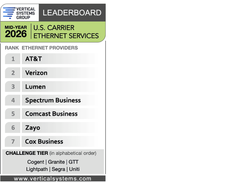
Vertical Systems Group’s (VSG’s) mid‑2026 U.S. Carrier Ethernet LEADERBOARD ranks providers by retail port share as of June 30, 2026. Seven network operators met the 4% threshold for Leaderboard status: AT&T; Verizon (including Frontier); Lumen; Spectrum Business; Comcast Business; Zayo (including Crown Castle); and Cox Business.
- Verizon’s acquisition of Frontier significantly expanded its fiber network, elevating its market position to #2 in the U.S. Carrier Ethernet rankings.
- Zayo advanced to the leaderboard after acquiring Crown Castle and plans to add 15,000 route miles by 2030, strengthening its long-haul network.
Six companies attained a Challenge Tier citation (in alphabetical order): Cogent, Granite, GTT, Lightpath, Segra, and Uniti. The Challenge Tier includes providers with between 1% and 4% share of the U.S. retail Ethernet market.
VSG’s methodology measures billable retail customer ports and segments the market into six service categories that map closely to MEF‑defined Carrier Ethernet service types: Ethernet DIA (Dedicated Internet Access), E‑Access to IP/MPLS VPN, Ethernet Private Line (EPL), Ethernet Virtual Private Line (EVPL), Metro LAN, and WAN VPLS.
U.S. Ethernet Market Analysis: Mid-2026:
- AT&T keeps its #1 rank on the Mid-Year 2026 U.S. Carrier Ethernet LEADERBOARD.
- Rankings change for four of the seven Ethernet LEADERBOARD providers.
- Verizon moves up from the #4 position to the #2 rank with its completed acquisition and integration of Frontier assets.
- As a result, Lumen dips from the #2 position to #3. Spectrum Business drops from #3 into the #4 position.
- Zayo moves up into the LEADERBOARD at the #6 position from the Challenge Tier due to its acquisition of Crown Castle, which was completed in May 2026.
- Cox Business falls into the #7 and final position. The acquisition of Cox by Spectrum’s parent company, Charter Communications, was completed in August 2026 and is not included in the mid-year results.
- The Challenge Tier for mid-2026 includes six companies: Cogent, Granite, GTT, Lightpath, Segra (including UPN) and Uniti (includes Windstream). Segra enters the Challenge Tier, moving up from the Market Player tier.
- DIA (Dedicated Internet Access) is the top Ethernet service in the U.S. based on both ports and revenue.
- Enterprise customers are shifting from lower speed Ethernet private lines to more robust SD-WAN and SASE services.
- Three LEADERBOARD wireline network operators have attained Mplify Carrier Ethernet certification: AT&T, Lumen and Verizon.
The Market Player tier includes all providers with port share below 1%. Companies in the Market Player tier include the following providers (in alphabetical order):ACD, AireSpring, Alaska Communications, Alta Fiber, American Telesis, Arelion, Armstrong Business Solutions, Astound Business, Bluebird Network (includes Everstream), Breezeline, Brightspeed, BT Global Services, Centracom, Conterra, Douglas Fast Net, DQE Communications, Epsilon, Exa Infrastructure, ExteNet Systems, Fatbeam, FiberLight, Fidium, First Digital, FirstLight, Flo Networks, Fusion Connect, GCI, GCX, Glo Fiber, Hunter Communications, Intelsat, Logix Fiber Networks, LS Networks, MetTel, Midco, Momentum Telecom, NTT, Orange Business, Pilot Fiber, PS Lightwave, Rightfiber (includes Great Plains and Ritter), Silver Star Telecom, Sparklight Business, Syringa, T-Fiber (includes MetroNet, Lumos, U.S. Internet), Tata Communications, TDS Telecom, TPx, US Signal, WOW!Business, Ziply Fiber (now owned by Bell Canada) and other companies selling retail Ethernet services in the U.S. market.
…………………………………………………………………………………………………………………………………………………………………………………………………………………………………….
Standards Context: MEF Carrier Ethernet, IEEE 802, and ITU-T:
Carrier Ethernet services are standardized by MEF (formerly the Metro Ethernet Forum), which defines service types, attributes, and performance objectives across multi‑operator domains. MEF 2.0/3.0 specifications formalize E‑Line (point‑to‑point), E‑LAN (multipoint), E‑Tree (rooted multipoint), and E‑Access (inter‑provider) services, with strict OAM, QoS, and bandwidth profile requirements.
At the physical and link layers, IEEE 802.3 Ethernet PHYs and 802.1Q VLAN tagging underpin these services, while MEF service definitions (EVCs, UNIs, ENNIs) provide the operator‑grade abstraction needed for SLAs, service multiplexing, and interconnection. In practice, “Metro Ethernet” offerings by U.S. carriers are implementations of MEF E‑Line/E‑LAN service types over diverse transport (packet optical, MPLS, IP/MPLS, or Ethernet switching fabrics), with port‑based or VLAN‑based handoffs at the customer UNI.
Metro Ethernet Service Types: What the Market Segments Map To:
Vertical’s six service segments align with canonical Carrier Ethernet service types as follows:
-
Ethernet DIA (Dedicated Internet Access): Typically delivered as an E‑Line service (EPL or EVPL) to an internet gateway, with asymmetric or symmetric bandwidth profiles and strict availability targets. DIA emphasizes internet reachability rather than private L2 connectivity, but the underlying UNI/EVC constructs remain MEF‑compliant.neosnetworks+1
-
E‑Access to IP/MPLS VPN: An inter‑provider or backhaul construct where a carrier Ethernet E‑Line/E‑Access link connects an enterprise edge or another operator to an IP/MPLS core. This maps to MEF E‑Access (inter‑carrier) with ENNI handoffs and is common for wholesale Ethernet backhaul and multi‑operator VPN aggregation.mplify+1
-
Ethernet Private Line (EPL): A port‑based, point‑to‑point E‑Line service with one EVC per UNI and near‑transparent frame delivery. EPL is the canonical “private line” for low‑latency, high‑certainty circuits between two sites, often used for data‑center interconnect or critical backhaul.
-
Ethernet Virtual Private Line (EVPL): A VLAN‑based E‑Line service that supports multiple EVCs on a single UNI via service multiplexing. EVPL enables point‑to‑point and point‑to‑multipoint topologies over shared access ports, improving port utilization and supporting multi‑service bundles (e.g., LAN + internet + VoIP) on one physical handoff.Metro LAN: A multipoint‑to‑multipoint E‑LAN service (sometimes called Ethernet Virtual Private LAN) that provides any‑to‑any Layer 2 connectivity among three or more sites. Metro LAN is the carrier analogue to VPLS and is widely used for campus interconnect, distributed enterprise LAN extension, and L2‑based application clustering.
-
WAN VPLS: A wide‑area VPLS instance delivering E‑LAN semantics across broader geographies, typically over MPLS cores. While MEF 3.0 emphasizes E‑LAN service attributes, many operators still market VPLS as the transport realization of E‑LAN for multi‑site Layer 2 domains.
The most important ITU‑T recommendations for Carrier Ethernet fall into three buckets: service definitions, OAM/fault & performance management, and protection/activation testing. Together they provide the operator‑grade framework that maps MEF service types (E‑Line, E‑LAN, E‑Tree, E‑Access) to measurable SLAs and resilient transport.itu+2
Core service definitions (what the service is):
-
G.8011/Y.1307 – Ethernet service framework
Defines the overall framework for Ethernet services (EVC/OVC/UNI/ENNI), service attributes, and OAM bindings. It is the ITU‑T umbrella that aligns with MEF service types and underpins EPL, EVPL, E‑LAN, E‑Tree, and E‑Access definitions. -
G.8011.1/Y.1307.1 – Ethernet Private Line (EPL)
Specifies EPL service attributes and parameters (port‑based, single EVC per UNI, bandwidth profiles, transfer characteristics). This is the canonical “private line” for point‑to‑point, low‑latency circuits.itu+1 -
G.8011.2/Y.1307.2 – Ethernet Virtual Private Line (EVPL)
Specifies EVPL service attributes (VLAN‑based, service multiplexing on a UNI, CIR/EIR/CBS/EBS). EVPL enables multiple services over one physical handoff while preserving SLA granularity. -
G.8011.3/Y.1307.3 – Ethernet LAN (E‑LAN)
Defines multipoint‑to‑multipoint E‑LAN service attributes (any‑to‑any L2 connectivity among ≥3 UNIs), the carrier analogue to VPLS and widely used for Metro LAN.scribd+1 -
G.8011.4/Y.1307.4 – Ethernet Virtual Private Rooted Multipoint (E‑Tree / EVPRM)
Defines rooted multipoint (E‑Tree) service attributes for hub‑and‑spoke topologies (e.g., video distribution, wholesale access). -
G.8011.5/Y.1307.5 – Ethernet Access (E‑Access)
Specifies inter‑provider Ethernet access service attributes (ENNI‑based) used for wholesale backhaul and multi‑operator service chaining
…………………………………………………………………………………………………………………………………………………………………………..
Market Implications for Network Architects:
The 2026 VSG leaderboard reflects consolidation and asset integration (e.g., Verizon’s move to #2 following Frontier integration), with cable MSOs and fiber specialists maintaining strong positions in metro and regional segments. For architects specifying Carrier Ethernet, the practical choice among EPL, EVPL, E‑LAN, and VPLS hinges on three factors: topology (P2P vs. multipoint), service multiplexing needs at the UNI, and the degree of L2 transparency versus managed L3 VPN requirements.
When drafting RFPs or architecture documents, reference:
- G.8011.x service types alongside MEF E‑Line/E‑LAN/E‑Tree/E‑Access to ensure interoperable, SLA‑backed procurement.
- MEF 2.0/3.0 service types (E‑Line/E‑LAN/E‑Access) and require conformance to MEF service attributes (bandwidth profiles, frame delay/jitter/loss, OAM).
That ensures that “Metro Ethernet” procurement aligns with deployable, interoperable, SLA‑backed services rather than vendor‑specific marketing terms.
…………………………………………………………………………………………………………………………………………….
References:
https://verticalsystems.com/2026/09/02/mid-2026-us-carrier-ethernet-leaderboard/
https://verticalsystems.com/methodology/
https://neosnetworks.com/resources/blog/epl-vs-evpl/
https://www.itbroker.com/resources/glossary/metro-ethernet-transport
Carrier Ethernet Market Assessment and MEF 3.0 Certification
AT&T Tops VSG 2022 Global Provider Carrier Managed SD-WAN Leaderboard
No Surprise: AT&T tops leaderboard of commercial fiber lit buildings for 7th year!
VSG LEADERBOARD : AT&T #1 in Fiber Lit Buildings- Year end 2020
AT&T tops VSG’s U.S. Carrier Managed SD-WAN Leaderboard for 4th year
Lumen Technologies tops Vertical Systems Group’s 2021 U.S. Wavelength Services Leaderboard
PwC: Global AI data center spending to hit $31.6tn by 2050; Role of full stack orchestration layer explained
The AI infrastructure boom is set to continue as per most market research firms. AI chip and compute server upgrade cycles will necessitate the continued spending of many hundreds of billions of dollars on AI compute infrastructure for the foreseeable future.
Global data center spending is set to reach US$31.6 trillion through 2050 to meet the world’s growing appetite for artificial intelligence (AI), an investment boom with no precedent in history, PricewaterhouseCoopers LLP (PwC) said in a report released on September 2, 2026. Dwarfing projects such as the railways, Internet and electrification, spending on data centers could even hit US$50 trillion over the next two-and-a-half decades if AI adoption accelerates beyond PwC’s “central scenario” forecast, the professional service/accounting firm said. For comparison, US GDP is about US$30 trillion.
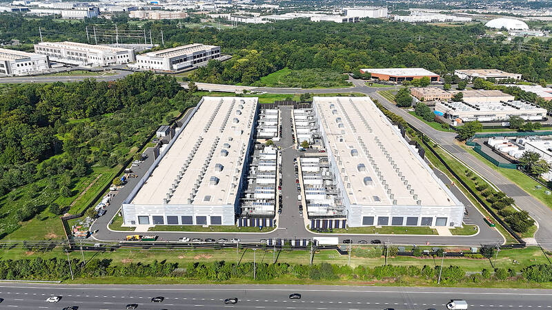
An Amazon Web Services data center in Sterling, Virginia. Photo: AFP
With consumers, companies and governments increasingly using AI, tech giants such as Microsoft Corp and Amazon.com Inc and smaller data center providers are setting up new computing facilities across the planet at a rapid clip. The bulk of the spending would go into what fills the data centers — hardware from companies such as AI chip leader Nvidia Corp.
At least 75 projects, worth about US$130 billion combined, were blocked or delayed by local opposition during the first three months of this year, according to research group Data Center Watch.
“AI infrastructure is becoming one of the defining capital allocation challenges of the next generation,” said Clara Cutajar, global infrastructure leader at PwC Australia. “It cuts across technology, energy, real estate, supply chains, regulation and financing. This changes how infrastructure investors need to think about capital requirements, risk and returns.”
At the same time, the tech industry is trying to blunt a backlash against data centers that threatens to slow down the buildout. Protesters cite concerns about environmental impacts, resource consumption and more broadly how AI could upend employment and society. The U.S. would capture nearly half the projected data center spending, at US$15.1 trillion, PwC said.
The Asia-Pacific region would follow at US$8.2 trillion, Europe at US$5.6 trillion, the Middle East at US$1.1 trillion and Africa at US$255 billion of the cumulative capital expenditure, PwC’s inaugural Global Data Center Outlook showed.
“Railways. Electrification. The Internet. Each required enormous amounts of capital and defined an era,” the researchers said in the report. “The AI infrastructure cycle under way dwarfs all three. This one resets every four to six years — and shows no signs of ending.”
On an annual basis, global data center spending would increase from about US$800 billion this year to US$1.1 trillion in 2030 and US$1.8 trillion in 2050, PwC predicted.
China and India would drive the largest share of incremental demand, supported by large populations, rapidly expanding digital economies, and substantial headroom for AI to embed in business and consumer activity.
While global demand is strong, factors such as power availability, data sovereignty requirements and the flow of semiconductors would determine which regions capture the investments, PwC said. Power would be the foremost factor that shapes where AI infrastructure investment occurs. Indeed, much of the forecast hinges on how fast reliable electricity supply for data centers can be established, the report said. Affordable, reliable, and increasingly low-carbon electricity at scale is the hardest requirement for many markets to meet.
While the market researchers’ projection assumes a fairly open trading system where chips move freely across borders, disruptions in semiconductor supply chains could cut global investment by nearly 20 percent, they said. Meanwhile, a growing sovereignty push could redistribute, but not reduce, global investment.
“The US$31.6 trillion question isn’t whether the capital exists. It does,” the researchers said. “Nor is the question whether the demand is real. It is. The question is which regions, operators and institutions are positioned to capture it and which aren’t.”
Analysis- Where Will the Money Come From?
OpenAI and Anthropic, the two poster-children for Western frontier AI development, routinely divulge soaring annualised revenue run-rates, but these only give a vague indication as to how things are actually going.
An LLM maker that has had a particularly good month can simply multiply that monthly figure by 12, resulting in a run rate that gives the impression that sales are booming. Two Bloomberg articles from August illustrate this distortion.
The first reveals that Anthropic’s actual revenue reached $11.5 billion in Q2, up from $4.73 billion in prior quarter, giving a total of $16.23 billion for the first half.
The second cites sources claiming Anthropic’s run-rate puts it on track to turn over $65 billion this year.
…………………………………………………………………………………………………………………………………….
Full Stack Orchestration Layer:
The pace and scale of an unprecedented data center buildout is leading to challenges across the infrastructure lifecycle. These challenges point to a need for a single accountable orchestration layer, one designed to manage the seams across the delivery stack. PwC refers to this role as a full-stack orchestrator, a delivery platform that sets the standards, manages the integrated schedule, governs risk and change, and defines how acceptance is measured across the project.
Key Takeaways:
- PwC estimates $5.1 trillion will be invested in data centers in the five years ending 2030 and around $32 trillion over the next 25 years depending on AI adoption.
- Turning that capital into usable megawatt capacity means overcoming the industry’s biggest delivery failures around power, equipment, cooling, construction, commissioning, and compute.
- A full-stack orchestrator can turn fragmented delivery into a repeatable platform by owning standards, schedules, risk, change control, and acceptance across the entire data center build.
…………………………………………………………………………………………………………………………………….
References:
https://www.taipeitimes.com/News/biz/archives/2026/09/04/2003863640
https://www.telecoms.com/ai/no-relief-in-sight-as-pwc-sees-ai-capex-reaching-31-6trn-by-2050
Big tech spending on AI data centers and infrastructure vs the fiber optic buildout during the dot-com boom (& bust)
AI Data Center Boom Carries Huge Default and Demand Risks
Expose: AI is more than a bubble; it’s a data center debt bomb
Will billions of dollars big tech is spending on Gen AI data centers produce a decent ROI?
How will fiber and equipment vendors meet the increased demand for fiber optics in 2026 due to AI data center buildouts?
China vs U.S.: Race to Generate Power for AI Data Centers as Electricity Demand Soars
AI Compute Has a Switchboard Problem: Orchestration & Data Center Fabric Explained
Nvidia CEO Huang: AI is the largest infrastructure buildout in human history; AI Data Center CAPEX will generate new revenue streams for operators
Analysis: Nvidia–MediaTek Deepen AI Platform Collaboration -What it Means for AI RAN & DCI
Executive Summary:
Nvidia has expanded its partnership with Taiwan based semiconductor firm MediaTek, committing $3.5 billion to a bond investment the two companies describe as a deepening of their “longstanding collaboration to build the next generations of AI computing platforms.” The move extends Nvidia’s pattern of strategic capital deployment across its compute ecosystem, this time reaching into custom silicon and advanced packaging.
According to the announcement, the collaboration couples Nvidia’s accelerated computing, AI, graphics, and software stack with MediaTek’s capabilities in custom silicon, high-performance computing (HPC), system-on-chip (SoC) design, and advanced packaging. MediaTek vice chairman and CEO Rick Tsai framed the investment as reinforcing a relationship spanning “cloud AI infrastructure, local AI computing and automotive in the era of physical AI,” combining Nvidia’s accelerated-computing and AI software ecosystem with MediaTek’s AI technology portfolio and custom-silicon resources.
Over the past several years, MediaTek has repositioned itself from a supplier of predominantly mid- and low-tier handset chipsets into a presence across smartphones, AI data centers, automotive, and IoT. Securities firm Yuanta Financial Holdings expects the closer alignment to accelerate MediaTek’s transition from edge AI into data-center infrastructure, device-based AI computing, and automotive platforms. Trading in MediaTek shares was suspended on the Taipei exchange Tuesday after the stock hit its daily 10% upside limit. The shares closed at NT$4,315 (about US$136.05), reflecting investor enthusiasm for the deepening of the collaboration.
NVIDIA and MediaTek are collaborating in three major areas:
- AI infrastructure: MediaTek will work with NVIDIA’s NVLink Fusion ecosystem to enable customers to develop custom AI infrastructure designed to integrate with NVIDIA rack-scale systems and AI factories.
- Local AI computing: The companies will continue to collaborate on multiple generations of NVIDIA RTX Spark™ and DGX Spark™ PC chips, powering consumer PCs, AI developer supercomputers and enterprise-class workstations, that integrate NVIDIA GPUs with MediaTek SoCs.
- Automotive: MediaTek and NVIDIA will continue developing platforms for AI-powered, software-defined vehicles in the era of physical AI.
“AI is transforming every computing platform — from the world’s largest AI factories to the PC and the car,” said Jensen Huang, founder and CEO of NVIDIA. “MediaTek is one of the world’s great semiconductor companies, with exceptional expertise in system-on-chip design, connectivity, leading performance and power efficiency. Together, we’re building platforms that bring NVIDIA accelerated computing to new markets and give customers the freedom to create differentiated AI systems at enormous scale.”
“MediaTek and NVIDIA share a vision for making advanced AI computing pervasive across the technology landscape,” said Rick Tsai, vice chairman and CEO of MediaTek. “NVIDIA’s investment strengthens a collaboration that spans cloud AI infrastructure, local AI computing and automotive in the era of physical AI. By combining NVIDIA’s leadership in accelerated computing and AI software ecosystem with MediaTek’s expertise in a diverse AI technology portfolio from edge to cloud, and our leadership position in custom silicon, we can accelerate innovation for our customers.”
Custom AI Infrastructure and NVLink Fusion:
Yuanta identified MediaTek’s participation in Nvidia’s NVLink Fusion as the most consequential element of the arrangement. Through that linkage, MediaTek could support the design of custom AI chips for clients while connecting them directly into Nvidia’s AI infrastructure — a complementary rather than competing role alongside the GPU vendor’s proprietary interconnect fabric.
The scale of the bond purchase also signals Nvidia’s long-term commitment to the relationship. Nvidia, currently the world’s most valuable company at roughly a $5 trillion market capitalization, has been deploying capital aggressively across both upstream and downstream partners. This latest deal, however, inevitably risks overlapping with other Nvidia investments — notably its $2 billion partnership with Marvell, which is also heavily oriented around NVLink Fusion and pitch-for the RAN with a one-chip architecture.
NVLink Fusion vs. Ethernet Scale-Out Interconnect:
NVLink Fusion and Ethernet-based scale-out interconnects target fundamentally different layers of the AI fabric, and the distinction turns on memory semantics rather than raw link rate. NVLink Fusion sits in the scale-up domain: it delivers memory-coherent, tightly coupled attachment for custom XPUs into Nvidia’s rack-scale NVLink fabric, with point-to-point GPU/XPU-to-GPU/XPU connectivity and an integrated high-bandwidth-memory interface (NVHBM) that trades die area and power for latency and bandwidth. It is proprietary, closed, and full-coherency by design — precisely the properties that make it hard for open standards to clone. Ethernet scale-out, by contrast, is the scale-out workhorse governing traffic between racks, pods, and clusters; it is loss-based, coarser-grained, and standardized through Ultra Ethernet and the broader IEEE 802.3 ecosystem.
The real contest is not NVLink against Ethernet so much as how much of the memory-coherent scale-up domain Ethernet-based challengers can capture. Standards-backed alternatives — UALink 2.0, Ultra Ethernet, and Broadcom’s Scale-Up Ethernet (SUE) — are pressing into scale-up territory, but they lack NVLink’s memory coherency and direct XPU-to-XPU connectivity, and SUE explicitly does not wire GPUs directly to GPUs. Meanwhile Nvidia’s strategy with NVLink Fusion is to co-opt custom XPUs (AWS Trainium4, and now MediaTek- and Marvell-designed silicon) into its fabric rather than let them migrate to those open scale-up paths. The practical outcome in the data center is a layered model — Ethernet surging in scale-out, and NVLink Fusion consolidating the latency-sensitive, memory-coherent scale-up spine — with Nvidia working to keep its proprietary layer the mandatory gateway that custom accelerators must pass through to reach the wider Ethernet-based world.
The $3.5 billion convertible-bond investment is best read not as a portfolio decision but as a defensive move within the AI rack-scale interconnect stack. The technical centerpiece is MediaTek’s adoption of the NVLink Fusion platform. Nvidia positions it as the connectivity technology and intellectual property that lets hyperscalers and AI-native operators drop custom accelerators (“XPUs”) and CPUs directly into its NVLink scale-up fabric.
MediaTek will now build against the three subsystems that define NVLink Fusion: the NVLink Fusion chiplet, which bridges a customer’s custom XPU to the NVLink scale-up domain over photonic or electrical interconnects (the chiplet itself carries up to ~1.8 TB/s of bidirectional bandwidth); NVLink-C2C, the high-bandwidth die-to-die link between XPUs, Nvidia’s Vera/Rosa CPUs, and other compatible processors; and NVHBM, a customized high-bandwidth-memory interface that trades off die area and power efficiency. The strategic significance is that Nvidia is effectively licensing its interconnect and memory layer as a licensable subsystem rather than enforcing a closed, all-Nvidia island — which lets it absorb “frenemy” silicon into the fabric instead of fighting it.
Two implications stand out for interconnect strategy:
-
A hedge on hyperscaler in-house silicon. AWS has already integrated its Trainium4 custom ASICs with NVLink Fusion for rack-scale deployment, and Google, Meta, Microsoft, and OpenAI are all advancing private accelerators. By standardizing the interface (NVLink Fusion, NVLink-C2C, NVHBM, chiplets, and rack-scale integration) that these custom XPUs must speak, Nvidia keeps chiplets, packages, memory, and racks—the connective infrastructure itself—inside its own revenue funnel. MediaTek, in turn, becomes the design conduit that helps hyperscalers and frontier model firms get to that tape-out without building an independent scale-up stack.
-
The scale-up vs. scale-out contest sharpens. NVLink remains essentially the only mature, memory-coherent scale-up fabric in production, whereas Ethernet is consolidating its dominance in scale-out (front-end and increasingly AI back-end) fabrics, and standards like Ultra Ethernet, UALink, and Broadcom’s Scale-Up Ethernet (SUE) are pressing into the scale-up domain. UALink and SUE, notably, lack NVLink’s memory coherency and point-to-point GPU-to-GPU connectivity, so NVLink Fusion’s positioning — co-opting custom XPUs rather than competing with them — lowers the attack surface those open standards could otherwise exploit.
The buy-in therefore consolidates Nvidia’s grip on the two layers that are hardest to commoditize: the latency-sensitive scale-up interconnect and the custom-silicon design flow that feeds it. What operators and chip partners give up is architectural independence — the bond structure and NVLink Fusion licensing effectively bind MediaTek into Nvidia’s ecosystem rather than allowing it to become an independent AI data-center silicon house.
What It Means for AI-RAN:
For the RAN, this is arguably a more consequential signal than the data-center economics. Nvidia’s AI-RAN play, via the AI Aerial software-defined accelerated-computing platform and its founding role in the AI-RAN Alliance, is built on having vRAN and AI workloads share the same GPU-accelerated infrastructure — what the community variously calls “AI for RAN,” “AI on RAN,” and “AI-and-RAN” on common hardware.nvidia+1
Here the MediaTek deal intersects directly with Nvidia’s earlier $2 billion Marvell partnership, which last year wired Marvell into the same NVLink Fusion platform for both the AI factory and AI-RAN ecosystem — Marvell supplying custom XPUs and NVLink Fusion-compatible scale-up networking, while Nvidia contributes the Vera CPU, ConnectX NICs, BlueField DPUs, Spectrum-X switches, and the rack-scale AI compute. The two arrangements are complementary in practice but overlapping in intent: Marvell owns the scale-up networking and the “one-chip-to-rule-the-RAN” custom silicon angle, while MediaTek brings SoC design, advanced packaging, and stronger reach into edge, automotive, and device-grade silicon. Together they give Nvidia two design houses capable of producing custom XPUs that plug into both data-center racks and AI-RAN infrastructure.
The operative question for IEEE readers is whether this broadens the AI-RAN supplier base going forward. Ericsson and Samsung have indicated their vRAN software built for Intel could be ported to AMD or Arm silicon with relatively modest effort, and Dell’Oro projections already have AI-RAN taking a significant share of the broader RAN market. Nvidia’s strategy is to ensure that, however the RAN silicon shakes out, the scale-up fabric and the custom-XPU design path remain NVLink Fusion-based — extending its data-center interconnect franchise into the radio access domain itself. The risk, flagged in the news report, is over-concentration: stacking Marvell and MediaTek onto the same NVLink Fusion foundation concentrates architectural leverage in Nvidia’s hands and could crowd out the open, multi-vendor fabric choices that O-RAN advocates would prefer to see served by standard Ethernet and UALink-style paths.
References:
https://www.lightreading.com/finance/nvidia-tips-3-5b-into-mediatek-in-latest-tech-partnership
Analysis: Nvidia’s $2 billion investment in Marvell; NVLink Fusion ecosystem & RAN vendor silicon strategy
Ericsson and MediaTek Demonstrate 3GPP-Based GNSS RTK Positioning with Sub-30cm Accuracy Over a Commercial 5G Network
5G infrastructure moves from coverage and speeds to cloud-native, orchestration, automation and AI-assisted networks
MediaTek overtakes Qualcomm in 5G smartphone chip market
AI Compute Has a Switchboard Problem: Orchestration & Data Center Fabric Explained
by Gaurav Sharma with Alan J Weissberger
Introduction:
Anthropic [1.] earned more revenue in the second quarter of 2026 than it did in all of 2025. The Claude AI maker company raked in $11.5 billion between April and June 2026, up from $787 million in the year-earlier quarter, $4.73 billion in Q1-2026 and up from ~ $10 billion for the entire previous year. CEO Dario Amodei told CNBC that the growth had been “just crazy” and “too hard to handle,” with demand far outstripping the company’s ability to build infrastructure with demand racing ahead of the company’s ability to scale infrastructure.
Anthropic is not alone. Bank of America projects that AI compute demand will outstrip supply through 2029. GPU lead times now stretch to 36–52 weeks.
Note 1. Anthropic is an American artificial intelligence startup founded by former OpenAI members that focuses on developing safety-oriented, steerable, and interpretable large language models like the Claude AI assistant.
This is happening even as the industry throws historic capital at capacity. Global data-center capital expenditure (capex) is on track to surpass $1 trillion in 2026, according to Dell’Oro Group. Yet the teams building with AI still cannot procure the compute they need, when they need it, at a price that lets them survive long enough to validate their thesis. The AI compute market has a switchboard problem — and fixing it calls for the same kind of thinking that transformed telecommunications.

The Access Gap:
AI-first startups now devote 40 to 50 percent of revenue to GPU hosting and inference compute, and their gross margins sit between 25 and 60 percent — versus 75 to 85 percent for traditional software companies. Compute has become the single largest cost line for most AI businesses, and it dictates what a team can afford to build.
Meanwhile, meaningful enterprise GPU capacity sits dormant. Teams hoard hardware for fear of losing access, locking accelerators into long-term reservations that sit underused overnight and between training runs. The capacity exists; the coordination does not.
The burden lands hardest on those who cannot afford the reservation game. Founders step down to cheaper hardware that slows their research. Teams cut experiments because they cannot secure enough accelerators. Projects stall while usable compute sits idle behind someone else’s contract. In this environment, access — not merit — decides which ideas reach the market and which never get tested.
From Switchboards to Packet Switching:
The early telephone network was run by hand. Every call required an operator to connect the subscriber — and each call claimed a dedicated circuit for its entire duration, even during silence. It worked, but it was slow, labor-intensive and wasteful.
GPU procurement works the same way today. An AI team identifies the hardware it wants, negotiates a reservation with a hyperscaler — AWS, Microsoft Azure or Google Cloud — and waits for capacity to become available. Each commitment locks a slice of the fleet to a single customer. The process is manual, slow and wasteful.
Telecommunications escaped this model in stages. Automated switching removed the operator; packet switching removed the dedicated circuit. Instead of reserving an entire line for one conversation, the network segmented each message into packets and routed them over whatever path had spare capacity, allowing many conversations to share a single trunk through statistical multiplexing. The same physical infrastructure carried far more traffic because capacity was allocated dynamically rather than reserved in advance.
AI compute needs an analogous shift: an orchestration plane that discovers available accelerators across multiple sources and routes each workload to suitable hardware — without the customer negotiating each connection individually.
It is already taking shape. Vendors are building orchestration systems that aggregate capacity from owned infrastructure, data centres and distributed GPU providers, then present it to the customer as a single service. The customer submits a job; the orchestration layer selects suitable hardware, assembles a cluster and delivers it.
Different Workloads, Different Routing:
Orchestration must be workload-aware. Pre-training the largest frontier models requires thousands of accelerators coupled over low-latency fabrics with precise topology; these jobs will continue to demand dense, purpose-built clusters.
Inference, fine-tuning and research are far more elastic. They tolerate geographic spread and run across a wider, more heterogeneous hardware pool. This mirrors how packet-switched networks treat traffic types differently while carrying them on shared infrastructure: a voice call needs bounded latency and continuity, while an email is routed over whatever path has spare capacity.
That differentiation opens the door for network operators. Data-centre operators and carriers already own much of the physical connectivity — fibre, points of presence, interconnection — needed to knit scattered compute into a coherent supply system. Rather than letting AI infrastructure consolidate into a small number of hyperscalers, the industry can use existing transport and edge assets to link regional data centres and GPU providers into a broader, more liquid market.
Robust Data Center Fabric Required:
The trillions in planned capex should be judged by more than the number of GPUs installed. If new capacity flows mainly to customers who can lock in multi-year reservations, the supply of compute grows even as the population of companies able to use it shrinks — fewer experiments, fewer competing hypotheses, a smaller set of teams shaping what AI becomes.
A healthier market would let AI teams reach compute from multiple providers through a single, well-connected service, with the network doing the work of matching each job to the right hardware — the telecoms discipline of statistical multiplexing applied to the GPU fleet.
Telecommunications offers the template. Every forward step it took made the same physical infrastructure serve more users. AI compute looks ready for the same move. The hardware is there, but is the network that connects it robust enough?
The physical network that connects AI compute servers (GPUs/TPUs) to each other and to high-performance storage is collectively called the Data Center Network (DCN) Fabric. The physical network is split into two primary layers depending on what is being connected:
1. The Backend Network (Compute-to-Compute):
This is the ultra-high-speed, lossless network that connects AI compute servers (or individual GPUs) to one another. It handles “East-West” traffic—such as gradient exchanges and parameter updates—during massive parallel AI training.InfiniBand: Long considered the gold standard for high-performance computing (HPC). It relies on dedicated, high-speed physical switches and host channel adapters (pioneered largely by NVIDIA/Mellanox). It features native Remote Direct Memory Access (RDMA), allowing systems to exchange data directly from memory to memory without involving the host CPU.AI-Optimized Ethernet (RoCEv2): A highly popular open alternative that uses traditional physical Ethernet cabling and switches but runs RDMA over Converged Ethernet (RoCEv2).
Platforms like NVIDIA Spectrum-X utilize optimized Ethernet hardware to achieve lossless, low-latency performance comparable to InfiniBand.Ultra Ethernet: Driven by the Ultra Ethernet Consortium (UEC), this next-generation physical transport standard optimizes Ethernet specifically for massive scale-out AI environments.
2. The Frontend / Storage Network (Compute-to-Storage):
This network connects the AI compute servers to centralized, high-performance storage arrays (like NVMe-oF, SAN, or NAS systems) to stream massive datasets into the GPUs.High-Speed Ethernet: The physical storage network is predominantly built on high-bandwidth Ethernet (moving rapidly up to 400G and 800G per port).Storage Protocols: It leverages protocols like NVMe-oF (NVMe over Fabrics) or RoCEv2 to pull unstructured data (images, text corpuses) from storage units into the compute cluster at lightning speeds without stalling the GPUs.
| Feature | InfiniBand Fabric | AI Ethernet (RoCEv2 / UEC) |
|---|---|---|
| Primary Use Case | Tightly coupled GPU-to-GPU training | Compute-to-Storage & open scale-out clusters |
| Physical Hardware | Dedicated, specialized switches & optics | Standard, widely available Ethernet switches |
| Data Flow Style | Lossless by design (Credit-based flow control) | Lossless via configuration (PFC / ECN mechanisms) |
| Ecosystem | Proprietary / Closed ecosystem | Open standard, multi-vendor interoperability |
………………………………………………………………………………………………………………………………………………….
References:
Telecom data centers must be redesigned for the AI era with rack scale architectures, enhanced power & cooling requirements
Analysis: Ethernet gains on InfiniBand in data center connectivity market; White Box/ODM vendors top choice for AI hyperscalers
Will AI clusters be interconnected via Infiniband or Ethernet: NVIDIA doesn’t care, but Broadcom sure does!
Cisco’s Silicon One G300 as the dominant AI networking fabric, competing with Broadcom’s Tomahawk 6 series
Big tech spending on AI data centers and infrastructure vs the fiber optic buildout during the dot-com boom (& bust)